MIT.nano equipment to accelerate innovation in “tough tech” sectors
by Zach Winn for MIT News
Boston MA (SPX) Feb 01, 2024
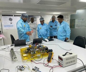
A new set of advanced nanofabrication equipment will make MIT.nano one of the world’s most advanced research facilities in microelectronics and related technologies, unlocking new opportunities for experimentation and widening the path for promising inventions to become impactful new products.
The equipment, provided by Applied Materials, will significantly expand MIT.nano’s nanofabrication capabilities, making them compatible with wafers – thin, round slices of semiconductor material – up to 200 millimeters, or 8 inches, in diameter, a size widely used in industry. The new tools will allow researchers to prototype a vast array of new microelectronic devices using state-of-the-art materials and fabrication processes. At the same time, the 200-millimeter compatibility will support close collaboration with industry and enable innovations to be rapidly adopted by companies and mass produced.
MIT.nano’s leaders say the equipment, which will also be available to scientists outside of MIT, will dramatically enhance their facility’s capabilities, allowing experts in the region to more efficiently explore new approaches in “tough tech” sectors, including advanced electronics, next-generation batteries, renewable energies, optical computing, biological sensing, and a host of other areas – many likely yet to be imagined.
“The toolsets will provide an accelerative boost to our ability to launch new technologies that can then be given to the world at scale,” says MIT.nano Director Vladimir Bulovic, who is also the Fariborz Maseeh Professor of Emerging Technology. “MIT.nano is committed to its expansive mission – to build a better world. We provide toolsets and capabilities that, in the hands of brilliant researchers, can effectively move the world forward.”
The announcement comes as part of an agreement between MIT and Applied Materials, Inc. that, together with a grant to MIT from the Northeast Microelectronics Coalition (NEMC) Hub, commits more than $40 million of estimated private and public investment to add advanced nano-fabrication equipment and capabilities at MIT.nano.
“We don’t believe there is another space in the United States that will offer the same kind of versatility, capability, and accessibility, with 8-inch toolsets integrated right next to more fundamental toolsets for research discoveries,” Bulovic says. “It will create a seamless path to accelerate the pace of innovation.”
Pushing the boundaries of innovation
Applied Materials is the world’s largest supplier of equipment for manufacturing semiconductors, displays, and other advanced electronics. The company will provide at MIT.nano several state-of-the-art process tools capable of supporting 150- and 200-millimeter wafers and will enhance and upgrade an existing tool owned by MIT. In addition to assisting MIT.nano in the day-to-day operation and maintenance of the equipment, Applied Materials engineers will develop new process capabilities to benefit researchers and students from MIT and beyond.
“This investment will significantly accelerate the pace of innovation and discovery in microelectronics and microsystems,” says Tomas Palacios, director of MIT’s Microsystems Technology Laboratories and the Clarence J. Lebel Professor in Electrical Engineering. “It’s wonderful news for our community, wonderful news for the state, and, in my view, a tremendous step forward toward implementing the national vision for the future of innovation in microelectronics.”
Nanoscale research at universities is traditionally conducted on machines that are less compatible with industry, which makes academic innovations more difficult to turn into impactful, mass-produced products. Jorg Scholvin, associate director for MIT.nano’s shared fabrication facility, says the new machines, when combined with MIT.nano’s existing equipment, represent a step-change improvement in that area: Researchers will be able to take an industry-standard wafer and build their technology on top of it to prove to companies it works on existing devices, or to co-fabricate new ideas in close collaboration with industry partners.
“In the journey from an idea to a fully working device, the ability to begin on a small scale, figure out what you want to do, rapidly debug your designs, and then scale it up to an industry-scale wafer is critical,” Scholvin says. “It means a student can test out their idea on wafer-scale quickly and directly incorporate insights into their project so that their processes are scalable. Providing such proof-of-principle early on will accelerate the idea out of the academic environment, potentially reducing years of added effort. Other tools at MIT.nano can supplement work on the 200-millimeter wafer scale, but the higher throughput and higher precision of the Applied equipment will provide researchers with repeatability and accuracy that is unprecedented for academic research environments. Essentially what you have is a sharper, faster, more precise tool to do your work.”
Scholvin predicts the equipment will lead to exponential growth in research opportunities.
“I think a key benefit of these tools is they allow us to push the boundary of research in a variety of different ways that we can predict today,” Scholvin says. “But then there are also unpredictable benefits, which are hiding in the shadows waiting to be discovered by the creativity of the researchers at MIT. With each new application, more ideas and paths usually come to mind – so that over time, more and more opportunities are discovered.”
Because the equipment is available for use by people outside of the MIT community, including regional researchers, industry partners, nonprofit organizations, and local startups, they will also enable new collaborations.
“The tools themselves will be an incredible meeting place – a place that can, I think, transpose the best of our ideas in a much more effective way than before,” Bulovic says. “I’m extremely excited about that.”
Palacios notes that while microelectronics is best known for work making transistors smaller to fit on microprocessors, it’s a vast field that enables virtually all the technology around us, from wireless communications and high-speed internet to energy management, personalized health care, and more.
He says he’s personally excited to use the new machines to do research around power electronics and semiconductors, including exploring promising new materials like gallium nitride, which could dramatically improve the efficiency of electronic devices.
Fulfilling a mission
MIT.nano’s leaders say a key driver of commercialization will be startups, both from MIT and beyond.
“This is not only going to help the MIT research community innovate faster, it’s also going to enable a new wave of entrepreneurship,” Palacios says. “We’re reducing the barriers for students, faculty, and other entrepreneurs to be able to take innovation and get it to market. That fits nicely with MIT’s mission of making the world a better place through technology. I cannot wait to see the amazing new inventions that our colleagues and students will come out with.”
Bulovic says the announcement aligns with the mission laid out by MIT’s leaders at MIT.nano’s inception.
“We have the space in MIT.nano to accommodate these tools, we have the capabilities inside MIT.nano to manage their operation, and as a shared and open facility, we have methodologies by which we can welcome anyone from the region to use the tools,” Bulovic says. “That is the vision MIT laid out as we were designing MIT.nano, and this announcement helps to fulfill that vision.”
Related Links
MIT.nano
Nano Technology News From SpaceMart.com
Computer Chip Architecture, Technology and Manufacture
- SEO Powered Content & PR Distribution. Get Amplified Today.
- PlatoData.Network Vertical Generative Ai. Empower Yourself. Access Here.
- PlatoAiStream. Web3 Intelligence. Knowledge Amplified. Access Here.
- PlatoESG. Carbon, CleanTech, Energy, Environment, Solar, Waste Management. Access Here.
- PlatoHealth. Biotech and Clinical Trials Intelligence. Access Here.
- Source: https://www.nanodaily.com/reports/MIT_nano_equipment_to_accelerate_innovation_in_tough_tech_sectors_999.html
- :is
- :not
- $UP
- 01
- 200
- 8
- a
- ability
- Able
- About
- academic
- academic research
- accelerate
- accessibility
- accommodate
- accuracy
- add
- added
- addition
- adopted
- advanced
- Agreement
- Aligns
- All
- allow
- Allowing
- also
- amazing
- an
- and
- Announcement
- Another
- anyone
- Application
- applied
- approaches
- architecture
- ARE
- AREA
- areas
- around
- Array
- AS
- assisting
- Associate
- At
- available
- barriers
- batteries
- BE
- because
- become
- before
- begin
- believe
- benefit
- benefits
- BEST
- Better
- between
- Beyond
- boost
- both
- boundaries
- brilliant
- build
- but
- by
- CAN
- cannot
- capabilities
- capability
- capable
- care
- chip
- Close
- coalition
- collaboration
- collaborations
- colleagues
- combined
- come
- comes
- commercialization
- committed
- Communications
- community
- Companies
- company
- compatibility
- compatible
- computing
- conducted
- could
- create
- creativity
- critical
- day-to-day
- designing
- designs
- develop
- device
- Devices
- different
- difficult
- directly
- Director
- discovered
- discovery
- displays
- do
- don
- dramatically
- driver
- each
- Early
- Effective
- effectively
- efficiency
- efficiently
- effort
- electrical engineering
- Electronic
- Electronics
- emerging
- Emerging Technology
- enable
- enables
- energy
- Engineering
- Engineers
- enhance
- entrepreneurs
- entrepreneurship
- Environment
- environments
- equipment
- essentially
- estimated
- Ether (ETH)
- excited
- existing
- Expand
- expansive
- experts
- explore
- Exploring
- exponential
- Exponential Growth
- extremely
- facilities
- Facility
- faster
- Feb
- field
- Figure
- fit
- fits
- For
- Forward
- from
- Fulfill
- fully
- fundamental
- future
- get
- given
- going
- grant
- Growth
- Hands
- Have
- he
- Health
- Health Care
- help
- helps
- hiding
- higher
- Highlight
- host
- HTML
- http
- HTTPS
- Hub
- i
- idea
- ideas
- imagined
- impactful
- implementing
- improve
- improvement
- in
- Inc.
- inception
- inches
- Including
- incorporate
- incredible
- industry
- industry partners
- innovate
- Innovation
- innovations
- inside
- insights
- integrated
- Internet
- into
- inventions
- investment
- IT
- ITS
- journey
- jpg
- Key
- Kind
- known
- laboratories
- laid
- largest
- launch
- lead
- leaders
- less
- like
- likely
- local
- Machines
- maintenance
- make
- MAKES
- Making
- manage
- management
- manufacturing
- many
- Market
- Mass
- mass-produced
- material
- materials
- means
- meeting
- methodologies
- million
- mind
- Mission
- MIT
- more
- most
- move
- much
- my
- nano
- National
- New
- new products
- New technologies
- news
- next
- next-generation
- nicely
- Nonprofit
- Nonprofit Organizations
- Notes
- of
- offer
- on
- ONE
- only
- open
- operation
- opportunities
- optical
- or
- organizations
- Other
- our
- out
- outside
- over
- owned
- Pace
- part
- partners
- path
- paths
- People
- Personalized
- Personally
- Place
- plato
- Plato Data Intelligence
- PlatoData
- potentially
- power
- precise
- Precision
- predict
- Predicts
- private
- process
- processes
- Produced
- Products
- Professor
- project
- promising
- prototype
- Prove
- provide
- provided
- providing
- public
- Push
- quickly
- rapidly
- RE
- reducing
- region
- regional
- related
- Renewable
- represent
- research
- Research Community
- researchers
- right
- round
- s
- same
- say
- says
- scalable
- Scale
- scientists
- seamless
- Sectors
- see
- semiconductor
- Semiconductors
- set
- several
- shared
- significantly
- Size
- small
- smaller
- So
- Space
- spx
- Startups
- State
- state-of-the-art
- States
- Step
- Student
- Students
- such
- supplement
- supplier
- support
- Supporting
- T
- Take
- tech
- Technologies
- Technology
- technology news
- test
- than
- that
- The
- The Future
- The State
- the world
- their
- Them
- themselves
- then
- There.
- These
- they
- thin
- Think
- this
- Through
- throughput
- time
- to
- today
- together
- tool
- tools
- toolsets
- top
- tough
- toward
- traditionally
- tremendous
- TURN
- United
- United States
- Universities
- unlocking
- unprecedented
- unpredictable
- upgrade
- us
- use
- used
- using
- usually
- variety
- Vast
- versatility
- View
- virtually
- vision
- wait
- Waiting
- want
- Wave
- Way..
- ways
- we
- welcome
- were
- What
- when
- which
- while
- WHO
- widely
- will
- wireless
- Wireless Communications
- with
- wonderful
- Work
- working
- works
- world
- years
- yet
- you
- Your
- zach
- zephyrnet