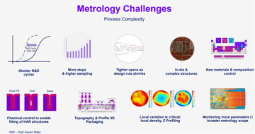
Overlay is becoming a significant problem in the manufacturing of semiconductors, especially in the world of advanced packaging substrates — think panels — the larger the area, the greater the potential for distortion due to warpage. Solving this issue requires more accurate models, better communication through feed forward/feed back throughout the flow, and real-time analytics that are baked into the process. Keith Best, director of product marketing for lithography at Onto Innovation, talks about the intricacies of overlay, the pros and cons of glass substrates, and what’s needed for high-volume manufacturing.
[embedded content]

- SEO Powered Content & PR Distribution. Get Amplified Today.
- PlatoData.Network Vertical Generative Ai. Empower Yourself. Access Here.
- PlatoAiStream. Web3 Intelligence. Knowledge Amplified. Access Here.
- PlatoESG. Carbon, CleanTech, Energy, Environment, Solar, Waste Management. Access Here.
- PlatoHealth. Biotech and Clinical Trials Intelligence. Access Here.
- Source: https://semiengineering.com/overlay-optimization-in-advanced-ic-substrates/
- :is
- 27
- 6
- 66
- 80
- a
- About
- accurate
- advanced
- All
- All Posts
- alternative
- analytics
- and
- ARE
- AREA
- At
- back
- baked
- becoming
- BEST
- Better
- chief
- Communication
- Cons
- content
- Director
- distortion
- due
- editor
- embedded
- Engineering
- especially
- flow
- For
- glass
- greater
- HTTPS
- in
- Innovation
- into
- intricacies
- issue
- jpg
- keith
- larger
- manufacturing
- Marketing
- models
- more
- needed
- of
- onto
- optimization
- packaging
- panels
- plato
- Plato Data Intelligence
- PlatoData
- Posts
- potential
- Problem
- process
- Product
- PROS
- real-time
- requires
- semiconductor
- Semiconductors
- significant
- Solving
- Talks
- text
- that
- The
- The Area
- the world
- Think
- this
- Through
- throughout
- thumbnail
- to
- world
- youtube
- zephyrnet
More from Semi Engineering

Automotive Safety: Having The Right Product Portfolio In Place
Source Node: 1868030
Time Stamp: Jan 4, 2023
Printed Electronics: Direct Flipchip Bonding of Ultra-Thin Chip On A Recently-Developed Stretchable Substrate
Source Node: 1994305
Time Stamp: Mar 5, 2023


Enabling New Server Architectures With The CXL Interconnect
Source Node: 2000742
Time Stamp: Mar 9, 2023

Universal Verification Methodology Coverage For Bluespec RISC-V Cores
Source Node: 2294503
Time Stamp: Sep 27, 2023


New Spintronics Manufacturing Process, Allowing Scaling Down To Sub-5nm (U. of Minnesota/NIST)
Source Node: 2022067
Time Stamp: Mar 20, 2023
Using Virtual Metal Fill To Predict The Impact Of High Level Nets
Source Node: 2270189
Time Stamp: Sep 14, 2023