Glass substrates are starting to gain traction in advanced packages, fueled by the potential for denser routing and higher signal performance than the organic substrates used today.
There are still plenty of problems to solve before this approach becomes mainstream. While glass itself is cheap and shares some important physical similarities to silicon, there are challenges with buildup, stress, and handling that still need to be worked out. In addition, data is sparse about behavior under different kinds of stresses that can affect performance and lifespan in real-world applications.
Nevertheless, the upside is significant, and progress is tangible. “Glass is getting close,” says Marc Jacobs, product management advisor at PDF Solutions. “Glass was pioneered by LCD displays and smart phone screens, and we realized if we can make wires and transistors on glass for LCDs, then we can replace printed circuit boards with them. Glass is really flat and has similar temperature coefficient of expansion to silicon — much better than other materials.”
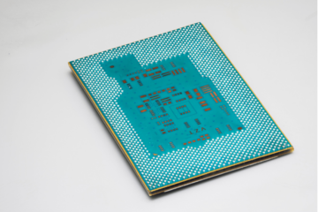
Fig. 1: Glass substrate test units at Intel’s Assembly and Test Technology Development factory. Source: Intel
With its superior flatness, insulation, and thermal properties, glass provides an attractive alternative to traditional substrates for emerging applications that require dense, high-performance interconnects. Yet, as is often the case with new materials, the industry’s understanding and methods must evolve concurrently with the adoption of the technology itself.
“Think about glass as a means to get interconnect density very similar to what you would get with silicon interposers,” says Rahul Manipali, fellow and director of substrate TD module engineering at Intel. “A glass substrate gives you that capability, but it comes with very challenging integration and interface engineering problems that we have to solve.”
Some of these challenges include fragility, a lack of adhesion to metal wires, and difficulties in achieving uniform via fill, which is crucial for consistent electrical performance. In addition, glass presents unique challenges for inspection and measurement, due to its high level of transparency and differing reflective indices compared to silicon. Many measurement techniques that work on opaque or semi-transparent materials are less effective on glass. For instance, optical metrology systems that rely on reflectivity to gauge distance and depth must adapt to glass’ translucency, which can cause signal distortion or loss, compromising measurement accuracy.
“All of these technologies assume certain physics,” says John Hoffman, computer vision engineering manager at Nordson Test & Inspection. “When you start changing substrates, will the physics still work? And can you recover? A lot of our algorithms make certain assumptions about the physics. Do those algorithms still work, or do we have to come up with brand new algorithms because the physics has changed?”
Lack of reliability data
Another critical hurdle in the widespread adoption of glass substrates is the scarcity of reliability data. Glass substrates are new entrants in the semiconductor packaging domain, and long-term reliability information is relatively scarce compared with traditional materials like FR4, polyimide or Ajinomoto Build-up Film (ABF), with decades of data used to establish standards, performance metrics, and lifespan expectations. For glass, the industry is still building that knowledge base. This data void raises concerns for applications where long-term performance and durability are paramount, such as in the automotive or aerospace sectors.
Reliability data for glass substrates encompasses a broad range of factors, including mechanical strength, thermal cycling resistance, moisture absorption, dielectric breakdown, and stress-induced delamination. Every one of these properties can profoundly impact the performance of the final product, especially under extreme or variable conditions.
“When you transition to a new substrate like glass, you’re essentially starting from scratch when it comes to reliability data,” says Keith Best, director of product marketing for lithography at Onto Innovation. “And you can’t move to high-volume manufacturing (HVM) unless you’ve got the reliability data.”
Furthermore, reliability is not only about the durability of the glass substrate itself, but also how well it interfaces with other materials in the packaging. Glass has excellent dimensional stability and can endure the thermal loads during chip packaging, but how it interacts with the solder or underfill materials over multiple thermal cycles, and how it maintains its adhesion to metal wires, are unknown.
The implications of this lack of data are significant. Without solid data, manufacturers may be hesitant to use glass substrates for high-reliability applications. Investment in the accelerated life testing of these materials, and the development of predictive models for their long-term behavior under stress, are essential.
Limited layers
The promise of glass substrates lies in the ability to support high-density interconnects, which are necessary for next-generation electronics. But this potential is currently curtailed by the practical constraints in the build-up process.
Silicon substrates and various types of laminates currently used in semiconductor packaging often allow for multiple layers of circuits, both on the top and the bottom, as well as internal layers. This layering is critical for achieving the required electrical pathways in multi-chip modules and complex integrated circuits. However, due to glass’s physical properties, such as its rigidity and the methods used for through-glass vias (TGVs), adding internal layers is problematic.
“You’re still severely limited in the number of layers that you can put on glass,” explains Dave Armstrong, director of business development at Advantest. “You can put a few layers on the top and a few layers on the bottom, but none in the middle. That’s going to be the fundamental limitation on it for the foreseeable future.”
This limited layering ability poses particular design challenges. Design engineers must find ways to route more connections through fewer layers, or develop new fabrication methods that allow for internal layering without compromising the substrate’s integrity. Such innovations could include new etching techniques, novel conductive materials for use with glass, or alternative methods of creating electrical interconnections.
The difficulty isn’t just about stacking the layers. It’s also about interconnecting them. In traditional substrates like ABF or copper clad laminate, vias are used to connect the circuit trace layers. With glass, the technologies to create these vias through multiple layers with the precision and reliability needed for semiconductor devices are still being refined.
“You can’t drill holes in ABF less than about 20 microns today,” notes Best. “And glass would be smaller. RDL requires smaller via holes, so we need a new photosensitive dielectric lacquer, or polyamide, or some sort of other material.”
Thermal expansion
One advantage with glass is its similar coefficient of thermal expansion to that of silicon, but glass also can exhibit markedly different thermal expansion coefficients when compared with other materials traditionally used in semiconductor devices.
This discrepancy in thermal behavior is critical during the assembly process, where precise temperature control is paramount. Semiconductor production encompasses a variety of thermal processes — from deposition, etching, and annealing to the solder reflow — a sequence during which materials are subjected to a broad spectrum of temperatures. Given the importance of maintaining dimensional stability, the mismatched thermal expansion rates of glass and other materials can lead to significant distortions and misalignments, particularly where uniform heating and cooling are difficult to ensure.
Consider, for instance, the stress and potential warping induced during a high-temperature solder reflow process. As devices undergo heating, parts expand and contract at rates defined by their thermal expansion coefficients. If glass substrates expand at a different rate to that of the chips or interconnects they host, stress can accumulate at the interfaces, risking the formation of micro-cracks or delamination.
“Sometimes test is the highest thermal stress a device will ever see, because you do scan patterns that aren’t representative of real workload,” says Mark Kahwati, product marketing director for semiconductor testing group at Teradyne. “The benefit of approaching that thermal balance is you can optimize throughput for test and minimize test cost, but you don’t want to get too far over the line that you’re introducing stress or latent defects.”
Precise metrology to measure and compensate for thermal effects on glass panels will be a vital aspect of quality control. Innovative thermal management solutions are being researched, including the use of conductive adhesives or underfill materials with matched thermal properties, new cladding techniques to distribute heat uniformly, or even the potential re-design of devices to accommodate for thermal expansion disparities.
Accurate thermal modeling and simulation also take on increased significance when working with glass. Designers and engineers must anticipate how glass substrates will interact with the rest of the package components in the thermomechanical environment of their operation. This extends from the microscale — looking at individual components — to the macroscale, considering whole device performance over its operational lifespan.
Stress and strain
In addition to thermal considerations, the physical stresses exerted on glass panels during the manufacturing process can induce strain within the material. The mechanical properties of glass, while lending to its flatness and rigidity, also make it susceptible to tensile and compressive forces that arise during processing. Understanding and measuring the stress distributions with glass is essential to ensure structural integrity.
For instance, the deposition of materials onto the glass substrate can introduce internal stresses due to the differing physical states of the substrate and the added layers. When these forces exceed the material’s inherent strength thresholds, it may lead to cracking or even complete substrate failure.
In addition, the stress introduced during the dicing and handling of glass substrates cannot be overlooked. The traditional sawing methods applied to more robust substrates often lead to chipping and fractures in glass. Consequently, manufacturers are exploring alternative dicing techniques, such as laser cutting. That promises to reduce mechanical stresses, but it requires precise control over laser parameters to avoid thermal stress accumulations.
Test and metrology tools must include capabilities for stress analysis. Raman spectroscopy offers a non-contact method to assess stress by measuring shifts in vibrational modes of the substrate’s molecules. Similarly, nanoindentation provides insights into the hardness and elastic modulus of the glass panels by applying controlled forces on a very small scale, thus minimizing the potential for additional surface damage.
Beyond the characterization and measurement of stress, managing these stresses in practice requires integration of stress-relieving steps into the manufacturing process. This could involve controlled temperature annealing, tailored to manage the thermal expansion characteristics of glass, or adding stress-compensating layers that would balance the inherent tensions within the material stack.
Glass advantages
Not all of the differences in glass from traditional substrates creates new challenges. The inherent transparency of glass substrates offers distinct advantages, including the integration of inspection techniques that were previously unfeasible with traditional, opaque substrates.
Infrared (IR) and X-ray imaging can be employed to non-destructively examine the inner workings of a glass-based electronic package. These methods enable the detection of sub-surface details, a capability that is particularly valuable for identifying imperfections or ensuring correct layer alignment without physically altering or damaging the component.
The optically clear nature of glass allows for more advanced forms of microscopy and scanning techniques. High-resolution optical inspection techniques can take full advantage of glass’s transparency, providing unprecedented views of device structures. It allows for the observation of processes like wire bond formation and solder joint creation in real-time.
“If you start to change to materials or substrates that are transparent, you might open up some optical techniques,” says Frank Chen, director of applications and product management at Bruker Nano Surfaces & Metrology. “That’s cheaper, faster and more mature. Whenever you can use optical, you go with optical.”
Glass’s stability also makes it an excellent candidate for precision-based metrology. Unlike materials that may warp or degrade over time, glass maintains its form, allowing for measurements that remain reliable in the long term. This consistency can ensure repeatable manufacturing processes and high yield rates.
For electronic packages that require RF transparency, glass’s dielectric properties make it a compelling choice. It enables the integration of antenna structures within the package itself without compromising signal integrity. This feature can lead to enhanced performance in wireless communication devices, where signal clarity and strength are critical.
Thermal imaging is another area where glass substrates excel. They allow for a more accurate assessment of heat distribution across a device due to their uniform thermal behavior. This can be crucial for thermal management strategies, facilitating better heat sink designs, and contributing to the overall reliability of electronic components.
Laser-based technologies that can measure slight variations in refractive index changes on glass surfaces can lead to new and improved ways of detecting stress patterns and deflections. Such precision could refine our understanding of material properties under operational conditions while contributing to better product designs that stand up to the rigors of everyday use.
While the transition to glass presents a range of challenges, it also opens up a realm of potential in testing and measurement. Advantages such as increased inspection capabilities, consistent metrology, RF transparency, and advanced thermal imaging align well with the broader industry goals of enhancing performance and ensuring reliability in semiconductor devices.
“There are some real inspection challenges with glass, but it’s still an emerging technology” says Brad Perkins, product line director at Nordson. “Still, it’s an exciting one, and it does solve some of the issues in advanced packaging.”
Conclusion
As industries increasingly push for more compact and complex devices, the demand for high-density, high-reliability packaging will continue to rise, and glass substrates will play a role in their advancement. While the challenges associated with integrating glass are significant, they are matched by considerable technological opportunities.
Glass substrates offer unparalleled flatness and thermal properties that are fundamental to the next generation of compact, high-performance packaging. The complexities encountered in manufacturing and testing glass are substantial, yet they are eclipsed by its potential advantages.
- SEO Powered Content & PR Distribution. Get Amplified Today.
- PlatoData.Network Vertical Generative Ai. Empower Yourself. Access Here.
- PlatoAiStream. Web3 Intelligence. Knowledge Amplified. Access Here.
- PlatoESG. Carbon, CleanTech, Energy, Environment, Solar, Waste Management. Access Here.
- PlatoHealth. Biotech and Clinical Trials Intelligence. Access Here.
- Source: https://semiengineering.com/glass-substrates-gain-foothold-in-advanced-packages/
- :has
- :is
- :not
- :where
- $UP
- 1
- 20
- a
- ability
- About
- accelerated
- accommodate
- Accumulate
- accuracy
- accurate
- achieving
- across
- adapt
- added
- adding
- addition
- Additional
- Adhesives
- Adoption
- advanced
- advancement
- ADvantage
- advantages
- advisor
- Aerospace
- affect
- algorithms
- align
- alignment
- All
- allow
- Allowing
- allows
- also
- alternative
- an
- analysis
- and
- Another
- antenna
- anticipate
- applications
- applied
- Applying
- approach
- approaching
- ARE
- AREA
- arise
- Armstrong
- AS
- aspect
- Assembly
- assess
- assessment
- associated
- assume
- assumptions
- At
- attractive
- automotive
- avoid
- Balance
- base
- BE
- because
- becomes
- before
- behavior
- being
- benefit
- BEST
- Better
- bond
- both
- Bottom
- brad
- brand
- Brand New
- Breakdown
- broad
- broader
- Building
- business
- business development
- but
- by
- CAN
- candidate
- cannot
- capabilities
- capability
- case
- Cause
- certain
- challenges
- challenging
- change
- changed
- Changes
- changing
- characteristics
- cheap
- cheaper
- chen
- chip
- Chips
- choice
- clarity
- clear
- Close
- come
- comes
- Communication
- compact
- compared
- compelling
- complete
- complex
- complexities
- component
- components
- compromising
- computer
- Computer Vision
- Concerns
- conditions
- Connect
- Connections
- Consequently
- considerable
- considerations
- considering
- consistent
- constraints
- continue
- contract
- contributing
- control
- controlled
- Copper
- correct
- Cost
- could
- cracking
- create
- creates
- Creating
- creation
- critical
- crucial
- Currently
- cutting
- cycles
- damage
- damaging
- data
- Dave
- decades
- defined
- Demand
- dense
- density
- depth
- Design
- designers
- designs
- details
- Detection
- develop
- Development
- device
- Devices
- differences
- different
- differing
- difficult
- difficulties
- Difficulty
- Director
- discrepancy
- displays
- distance
- distinct
- distribute
- distribution
- distributions
- do
- does
- domain
- Dont
- due
- durability
- during
- Effective
- effects
- Electronic
- Electronics
- emerging
- employed
- enable
- enables
- encompasses
- Engineering
- Engineers
- enhanced
- enhancing
- ensure
- ensuring
- entrants
- Environment
- especially
- essential
- essentially
- establish
- Ether (ETH)
- Even
- EVER
- Every
- everyday
- evolve
- examine
- exceed
- Excel
- excellent
- exciting
- exhibit
- Expand
- expansion
- expectations
- Explains
- Exploring
- extends
- extreme
- facilitating
- factors
- factory
- Failure
- far
- faster
- Feature
- fellow
- few
- fewer
- Fig
- fill
- Film
- final
- Find
- flat
- foothold
- For
- Forces
- foreseeable
- form
- formation
- forms
- fragility
- frank
- from
- fueled
- full
- fundamental
- future
- Gain
- gauge
- generation
- get
- getting
- given
- gives
- glass
- Go
- Goals
- going
- got
- Group
- Handling
- Have
- Hesitant
- High
- High Yield
- high-performance
- high-resolution
- higher
- highest
- Holes
- host
- How
- However
- HTTPS
- hurdle
- identifying
- if
- Imaging
- Impact
- implications
- importance
- important
- improved
- in
- include
- Including
- increased
- increasingly
- index
- Indices
- individual
- industries
- industry
- industry’s
- information
- inherent
- innovations
- innovative
- insights
- instance
- integrated
- Integrating
- integration
- integrity
- Intel
- interact
- interacts
- interconnecting
- interconnects
- Interface
- interfaces
- internal
- into
- introduce
- introduced
- introducing
- investment
- involve
- issues
- IT
- ITS
- itself
- John
- joint
- just
- keith
- knowledge
- Lack
- laser
- layer
- layering
- layers
- LCD
- lead
- lending
- less
- Level
- lies
- Life
- lifespan
- like
- limitation
- Limited
- Line
- loads
- Long
- long-term
- looking
- loss
- Lot
- Mainstream
- maintaining
- maintains
- make
- MAKES
- manage
- management
- manager
- managing
- Manufacturers
- manufacturing
- many
- mark
- Marketing
- Marketing Director
- matched
- material
- materials
- mature
- max-width
- May..
- means
- measure
- measurement
- measurements
- measuring
- mechanical
- metal
- method
- methods
- Metrics
- Metrology
- Microscopy
- Middle
- might
- minimize
- minimizing
- modeling
- models
- modes
- module
- Modules
- more
- move
- much
- multiple
- must
- nano
- Nature
- necessary
- Need
- needed
- New
- next
- next-generation
- None
- Notes
- novel
- number
- observation
- of
- offer
- Offers
- often
- on
- ONE
- only
- onto
- opaque
- open
- opens
- operation
- operational
- opportunities
- optical
- Optimize
- or
- organic
- Other
- our
- out
- over
- overall
- package
- packages
- packaging
- panels
- parameters
- Paramount
- particular
- particularly
- parts
- pathways
- patterns
- performance
- Perkins
- phone
- physical
- Physically
- Physics
- pioneered
- plato
- Plato Data Intelligence
- PlatoData
- Play
- Plenty
- poses
- potential
- Practical
- practice
- precise
- Precision
- predictive
- presents
- previously
- problems
- process
- processes
- processing
- Product
- product management
- Production
- profoundly
- Progress
- promise
- promises
- properties
- provides
- providing
- Push
- put
- quality
- raises
- range
- Rate
- Rates
- real
- real world
- real-time
- realized
- really
- realm
- Recover
- reduce
- refine
- refined
- relatively
- reliability
- reliable
- rely
- remain
- repeatable
- replace
- representative
- require
- required
- requires
- Resistance
- REST
- Rise
- risking
- robust
- Role
- Route
- routing
- says
- Scale
- scan
- scanning
- Scarce
- Scarcity
- scratch
- screens
- Sectors
- see
- semiconductor
- Sequence
- severely
- Shares
- Shifts
- Signal
- significance
- significant
- Silicon
- similar
- similarities
- Similarly
- simulation
- small
- smaller
- smart
- So
- solid
- Solutions
- SOLVE
- some
- Source
- Spectroscopy
- Spectrum
- Stability
- stack
- stacking
- stand
- standards
- start
- Starting
- States
- Steps
- Still
- strategies
- strength
- stress
- structural
- structures
- substantial
- such
- superior
- support
- Surface
- susceptible
- Systems
- tailored
- Take
- tangible
- TD
- techniques
- technological
- Technologies
- Technology
- Technology Development
- tensions
- term
- test
- Testing
- than
- that
- The
- their
- Them
- then
- There.
- thermal
- These
- they
- this
- those
- Through
- throughput
- Thus
- time
- to
- today
- too
- tools
- top
- trace
- traction
- traditional
- traditionally
- transition
- Transparency
- transparent
- types
- under
- undergo
- understanding
- unique
- units
- unknown
- unlike
- unparalleled
- unprecedented
- Upside
- use
- used
- Valuable
- variable
- variations
- variety
- various
- very
- via
- views
- vision
- vital
- want
- was
- ways
- we
- WELL
- were
- What
- when
- whenever
- which
- while
- whole
- widespread
- will
- Wire
- wireless
- with
- within
- without
- Work
- worked
- working
- workings
- would
- x-ray
- yet
- Yield
- you
- zephyrnet