Semiconductor Engineering sat down to discuss heterogeneous integration with Dick Otte, president and CEO of Promex Industries; Mike Kelly, vice president of chiplets/FCBGA integration at Amkor Technology; Shekhar Kapoor, senior director of product management at Synopsys; John Park, product management group director in Cadence‘s Custom IC & PCB Group; and Tony Mastroianni, advanced packaging solutions director at Siemens Digital Industries Software. What follows are excerpts of that conversation.
![[L-R] Dick Otte, president and CEO of Promex Industries; Mike Kelly, vice president of advanced packaging development and integration at Amkor Technology; John Park, product management group director in Cadence's Custom IC & PCB Group; Shekhar Kapoor, senior director of product management at Synopsys; and Tony Mastroianni, advanced packaging solutions director at Siemens Digital Industries Software.](https://platoaistream.net/wp-content/uploads/2023/10/heterogeneous-integration-finding-its-footing.png)
![[L-R] Dick Otte, president and CEO of Promex Industries; Mike Kelly, vice president of advanced packaging development and integration at Amkor Technology; John Park, product management group director in Cadence's Custom IC & PCB Group; Shekhar Kapoor, senior director of product management at Synopsys; and Tony Mastroianni, advanced packaging solutions director at Siemens Digital Industries Software.](https://platoaistream.net/wp-content/uploads/2023/10/heterogeneous-integration-finding-its-footing.png)
[L – R] Dick Otte, Mike Kelly, John Park, Shekhar Kapoor, and Tony Mastroianni.
SE: How do you define heterogeneous integration, and how has it changed? Is this just chiplets? Is it SoCs? Or is it 3D-ICs?
Park: We have done heterogeneous integration and packaging for decades with multi-chip modules, and eventually systems-in-packages. We didn’t call it heterogeneous integration, but that’s what we were doing. We didn’t use that term in the packaging world until people started disaggregating their chips, whether it was for yield, cost, or form factor. There are lots of things that come into play with people wanting to disaggregate the chip into multiple building blocks, and being able to design those building blocks in whatever process node or technology made the most sense. And then we aggregate it in the packaging world after the fact. Someone who traditionally would have approached their design as a monolithic chip is now approaching their design as a package that has multiple chiplets on it. They’re exploding that die into these different building blocks called chiplets. The integration of those chiplets across different technologies is what I call heterogeneous integration.
Kelly: Heterogeneous integration is the superset. A chiplet is a functional block that’s pulled out of what could have been an integrated monolithic die, and now it’s a chiplet. Whether that’s the I/O block or some piece of compute, those can be chiplets. Heterogeneous integration is a broader term. We started with MCMs a long, long time ago, with heterogeneous integration of dissimilar components in a single package.
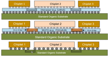
Kapoor: In today’s world, heterogeneous integration is putting together many pieces into a single advanced package. Those pieces could be varying kinds of pieces, not just silicon dies. They could be II-VI or III-V compound dies. So you can bring silicon and photonics together, and different kinds of materials together, all in one package. The term is expanding in that sense. In the past, with 2.5 D, when we were we talking about different die and HBM, we would not call that heterogeneous integration. People would just call it a silicon interposer design. It’s now coming under this one umbrella of advanced packaging, which could be 2.5D, fan-out, or 3D-IC. But if you’re integrating any of the pieces together, that’s all heterogeneous integration. The modes of integration could be different, but it’s still mixing technologies into one package.
Otte: Heterogeneous integration is a term that has come into broader use in contemporary times as we take more functionality and move it upstream, closer to the fab, in our packaging technologies. A lot of these functionalities that are now being added closer to the chip level used to be added at the circuit board level or the box level. Now we’re adding them on an interposer or chip-on-chip kinds of things. Pulling all of these non-silicon parts upstream, closer to the die, is a good way to describe that trend here. Originally it meant doing things like utilizing indium phosphide with CMOS, for example, but that quickly spread downstream. Now when you add an optical component with a CMOS device, some people are calling that heterogeneous integration.
Mastroianni: I define a chiplet as an IC that’s been designed and integrated, or designed and optimized to be integrated into a package. Integration of those chiplets is heterogeneous integration, whether that’s 2.5D or 3D-IC. Heterogeneous implies different technologies. They can be all silicon, but developed at different technology nodes. In some of the work we’re doing with DARPA, they’re defining heterogeneous integration as mixing silicon and non-silicon, so type III and V. Heterogeneous can be extended to either multiple ASIC technologies in silicon, but non-silicon technologies, as well. So it’s really having chiplets that are designed to be integrated in the package. And that’s the difference between traditional MCMs. HBM is not a true chiplet, but it really did launch the whole 2.5D approach. They’re connected together with standard interfaces, such as UCIe and BoW. HBM was like a very specialized chiplet that was designed with a very custom and standardized interface and HBM interface, so it’s like an off-the-shelf chiplet and a commercial part. If you step back a little bit, anybody doing these types of designs today, where multiple custom chips are being integrated, is doing multiple custom designs, which is a very expensive proposition. For this to get larger adoption throughout the industry, we need more standard off-the-shelf types of components like HBMs, and we need an ecosystem to support that.
SE: Where are you seeing the heterogeneous integration working best, and what makes that successful? Is it strictly more functions per design, because now we’re exceeding the reticle limits and there is no other way to do that? Or are there other benefits here?
Park: I’m seeing heterogeneous integration in these large, vertically integrated companies, like the big processor companies, where they have the resources to develop their own chiplets. There’s the advantage of reuse for them. They aren’t necessarily sharing those chiplets with the outside world, but they are taking advantage of it for reuse purposes. They can separate out parts of the logic that do not scale, like I/O and analog/RF. There’s no reason to scale those parts down to 5nm or 3nm when they can be designed at 28nm. That saves you money, and you can re-use them. That’s one area. There are lots of others that have to do with exotic form factors, like for products that get put in the human body. Heterogeneous integration is not what DARPA originally envisioned. There is no storefront or catalog of commercially available chiplets, which was the goal of the DARPA CHIPS program. We’re still working toward that.
Kapoor: The silicon interposer with 2.5D, which is where HBM has been used, has been there for a few years. That’s an example of heterogeneous integration. There also are all these HPC data center designs where you split out the cache and have the memory sitting right on the logic. That’s an example where you have high compute needs that’s working. There are many, many HPC companies moving in that direction. Those are the primary ones that are coming to the fore. And then there are some consumer applications, like a CMOS image sensor, where you have a transistor logic die and a photo-diode sensor die. The form factor pushes them to do heterogeneous integration. Automotive is also good example. Different tiers are starting to do silicon designs themselves. That’s where the whole ecosystem resilience, the drivers, come into the play, so can we have all these dies made available to do chiplet-based design. It’s an emerging area, but we’re beginning to see that heterogeneous integration could work very well with this approach, based on the dynamics of a particular market segment or vertical.
Otte: We see two places where what heterogeneous integration has been successful. One is in the optical space, where conventional CMOS devices are combined with photonic integrated circuits. They’ve got waveguides and lasers on them. The second place we’ve seen it is in biotech, where people take silicon wafers at 12 inches and put different chemistries on the wafer. And then they build further on that and ultimately utilize optical or electronic techniques to analyze fluids that are run across the surface of the chip. From our perspective, we refer to that as heterogeneous integration, too, but it begins to stretch the term. It’s a long way from where it originally started.
Kapoor: We also see the same thing. Co-packaged optics is another area, where data center traffic comes into play. We’re seeing all these compound semiconductors.
Kelly: That’s really broadening the horizon for what could be called heterogeneous, and it’s exciting. Looking back on what we’ve been working on recently, one thing that has worked well is getting DRAM into the package. Lowering the power from processor to DRAM really freed up a power budget that could be spent in grabbing more performance. That was one good thing. If you’re into gaming and graphics, and 3D CAD, that was a pretty big deal. But the biggest benefit we’ve seen is that chiplets has enabled compute, in all of its many forms, to increase performance in these newer nodes at a cost that’s still acceptable. That is a really big deal for our industry, because you can’t design a huge 3nm die affordably. It has to be broken up into components that make more sense, so you spend the 3nm FETs on something that has to have it. So DRAM getting close, and using chiplets to stay on a performance-per-dollar curve or line makes sense for our industry.
Mastroianni: If we look at what’s working best, I would say HBM-based designs. At this point, that is a mature technology. All the standards are there for integrating that technology. Silicon interposers are pretty straightforward. There are many applications that can leverage having memory right next to the chip. In that case, you’re typically just designing one custom chip and some interfaces. We’re seeing broader adoption of that by more and more companies. It’s becoming approachable. And then there’s the high-performance compute and AI type applications where the big processor companies are stacking memories and doing very sophisticated, very custom chips. That’s very successful, but it’s very expensive. The companies building those huge systems and very complex systems can afford to do that, and they’re getting the benefits financially from that. There is some sense of 3D, but it’s more of a stacked-die manual approach. The other type of 3D that people are doing today are sensor-type chips, where they’re stacking sensors on top of memories and processors. True 3D is still out there, and that’s going to need the tools to catch up to be able to take a very large system, decompose that into multiple chiplets, and then place-and-route it. It’s not there today, but once that technology becomes available, it’s is going to become more widely adopted.
Related Reading
Chiplets: 2023 (EBook)
Dig into what chiplets are, what they’re being used for today, and what they’ll be used for in the future with a look at hurdles, technologies, and standards.
Mini-Consortia Forming Around Chiplets
Commercial chiplet marketplaces are still on the distant horizon, but companies are getting an early start with more limited partnerships.
- SEO Powered Content & PR Distribution. Get Amplified Today.
- PlatoData.Network Vertical Generative Ai. Empower Yourself. Access Here.
- PlatoAiStream. Web3 Intelligence. Knowledge Amplified. Access Here.
- PlatoESG. Carbon, CleanTech, Energy, Environment, Solar, Waste Management. Access Here.
- PlatoHealth. Biotech and Clinical Trials Intelligence. Access Here.
- Source: https://semiengineering.com/heterogeneous-integration-finding-its-footing/
- :has
- :is
- :not
- :where
- $UP
- 1
- 12
- 2023
- 3d
- a
- Able
- About
- acceptable
- across
- add
- added
- adding
- adopted
- Adoption
- advanced
- ADvantage
- afford
- After
- aggregate
- ago
- AI
- All
- also
- an
- analyze
- and
- Another
- any
- applications
- approach
- approaching
- ARE
- AREA
- around
- AS
- asic
- At
- automotive
- available
- back
- based
- BE
- because
- become
- becomes
- becoming
- been
- Beginning
- being
- benefit
- benefits
- BEST
- between
- Big
- Biggest
- biotech
- Bit
- Block
- Blocks
- board
- body
- Box
- bring
- broader
- Broken
- budget
- build
- Building
- but
- by
- cache
- CAD
- Cadence
- call
- called
- calling
- CAN
- case
- catalog
- Catch
- Center
- ceo
- changed
- chip
- Chips
- Close
- closer
- combined
- come
- comes
- coming
- commercial
- commercially
- Companies
- complex
- component
- components
- Compound
- Compute
- connected
- consumer
- contemporary
- conventional
- Conversation
- Cost
- could
- curve
- custom
- darpa
- data
- Data Center
- deal
- decades
- define
- defining
- describe
- Design
- designed
- designing
- designs
- develop
- developed
- Development
- device
- Devices
- DID
- Die
- difference
- different
- digital
- direction
- Director
- discuss
- Distant
- do
- doing
- done
- down
- drivers
- dynamics
- Early
- eBook
- ecosystem
- either
- Electronic
- emerging
- enabled
- Engineering
- Ether (ETH)
- eventually
- example
- exciting
- Exotic
- expanding
- expensive
- fact
- factor
- factors
- few
- financially
- finding
- follows
- For
- for yield
- fore
- form
- forms
- from
- functional
- functionalities
- functionality
- functions
- further
- future
- gaming
- get
- getting
- goal
- going
- good
- got
- graphics
- Group
- Have
- having
- here
- High
- high-performance
- horizon
- How
- hpc
- HTTPS
- huge
- human
- Hurdles
- i
- if
- iii
- image
- in
- inches
- Increase
- industries
- industry
- integrated
- Integrating
- integration
- Interface
- interfaces
- into
- IT
- ITS
- John
- just
- Kapoor
- large
- larger
- lasers
- launch
- Level
- Leverage
- like
- Limited
- limits
- Line
- little
- logic
- Long
- long time
- Look
- looking
- Lot
- lots
- lowering
- made
- make
- MAKES
- management
- manual
- many
- Market
- marketplaces
- materials
- mature
- max-width
- meant
- Memories
- Memory
- mike
- Mixing
- modes
- Modules
- money
- Monolithic
- more
- most
- move
- moving
- multiple
- necessarily
- Need
- needs
- newer
- next
- no
- node
- nodes
- now
- of
- on
- once
- ONE
- ones
- optical
- optics
- optimized
- or
- originally
- Other
- Others
- our
- out
- outside
- own
- package
- packaging
- Park
- part
- particular
- partnerships
- parts
- past
- People
- per
- performance
- perspective
- piece
- pieces
- Place
- Places
- plato
- Plato Data Intelligence
- PlatoData
- Play
- Point
- power
- president
- pretty
- primary
- process
- Processor
- processors
- Product
- product management
- Products
- Program
- proposition
- pulling
- purposes
- pushes
- put
- Putting
- quickly
- R
- really
- reason
- recently
- refer
- resilience
- Resources
- reuse
- right
- Run
- s
- same
- say
- Scale
- Second
- see
- seeing
- seen
- segment
- Semiconductors
- senior
- sense
- sensors
- separate
- sharing
- Siemens
- Silicon
- single
- Sitting
- So
- Software
- Solutions
- some
- Someone
- something
- sophisticated
- Space
- specialized
- spend
- spent
- split
- spread
- stacking
- standard
- standardized
- standards
- start
- started
- Starting
- stay
- Step
- Still
- Storefront
- straightforward
- successful
- such
- support
- Surface
- system
- Systems
- Take
- taking
- talking
- techniques
- Technologies
- Technology
- term
- that
- The
- The Future
- their
- Them
- themselves
- then
- There.
- These
- they
- thing
- things
- this
- those
- throughout
- time
- times
- to
- today
- today’s
- together
- Tony
- too
- tools
- top
- toward
- traditional
- traditionally
- traffic
- Trend
- true
- two
- type
- types
- typically
- Ultimately
- umbrella
- under
- until
- use
- used
- using
- utilize
- Utilizing
- varying
- vertical
- vertically
- very
- vice
- Vice President
- wanting
- was
- Way..
- we
- WELL
- were
- What
- whatever
- when
- whether
- which
- WHO
- whole
- widely
- with
- Work
- worked
- working
- world
- would
- years
- Yield
- you
- zephyrnet


