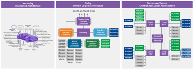
The automotive industry continues to evolve the centralized electrical/electronic (EE) architecture, impacting automakers, and Tier 1 and Tier 2 suppliers, as they implement various applications over the next 10 years. The new architecture is structured around a centralized compute module which executes multiple applications such as Advanced Driver Assistance Systems (ADAS)/highly automated driving (HAD), infotainment, chassis/body control and powertrain. The new centralized EE architecture is creating a new generation of system-on-chips (SoCs) with increased levels of integration, very high performance, and increased amounts of AI to host the combined applications. This article highlights the trend towards an integrated ADAS/IVI application enabled by a centralized compute SoC implementing automotive-grade interface and processor IP.

Fig. 1: Evolution of electrical/electronic (EE) system architectures.
Advantages of integrating multiple automotive applications in a single SoC
Combining ADAS and digital cockpit (or IVI) functionality requires the simultaneous execution of ADAS applications such as automatic emergency braking (AEB), adaptive cruise control, and lane keep aid (LKA) with the digital cockpit applications such as pillar-to-pillar high resolutions displays. The automotive industry’s decision to merge applications into integrated HW may occur incrementally, targeting multiple different hybrid approaches. A different combination of merged applications for a centralized EE architecture could be to merge telematics functions with ADAS functions, or multiple different hybrid platforms integrating different applications. Such integrations can create new opportunities for both HW and SW suppliers.
The implementation of zonal architectures with a centralized compute module will impact the compute SoCs that host the merged applications. The new generation of central compute SoCs running multiple applications require increased levels of AI processing, increased numbers of cache coherent multi-core 64-bit host processors, and increased levels of display processing. Due to the high performance and complexity to implement the compute SoCs, advanced semiconductor finFET processes are required. Integrating multiple functions into a central compute SoC will lower cost and minimize complexity, allowing automakers, Tier 1, and Tier 2 suppliers to differentiate.
Central computer SoC requirements
The new generation of automotive central compute SoCs will have common criteria, including high amounts of sensor data transported along the in-car network and high amounts of AI using the latest AI algorithms.
The high amounts of sensor data for safety critical ADAS applications must be continuously processed in real time. Data from sensors such as radar, lidar, ultrasonic, and camera sensors need to continuously arrive with the lowest latency. The data traffic and protocols must not oversubscribe the in-car network wiring harness. Most in-car networks using a combination of automotive grade Ethernet, direct connect MIPI links for image sensors, and legacy CAN networks. Due to the amount of radar/lidar data running over automotive grade Ethernet, multiple streams of 10G Ethernet are required for the Ethernet links using the IEEE Ethernet Time Sensitive Networking (TSN) protocol. By using the Ethernet TSN protocol, high priority safety-critical data packets can be transferred based on network policies to ensure lower priority data such as rear-seat entertainment does not interfere with safety-critical applications. For imaging data, a high-resolution image sensor can generate over 10G of real-time uncompressed data per sensor, which would overload the Ethernet network carrying the radar/lidar data. As such, most imaging data is transported using a separate MIPI interface. Several proprietary protocols have been developed to transfer MIPI-based imaging data in the severe channel conditions in the car. In addition to proprietary data channels, the MIPI Alliance has developed the new 15m automotive A-PHY protocol to carry image data to central compute modules. MIPI A-PHY is becoming more popular as an in-car data transfer protocol.
The new generation of centralized compute SoCs must execute real-time, simultaneous applications. Since multiple real-time applications are running simultaneously, the processing SoCs used in the centralized compute modules must support virtualization similar to high performance data center server processors. Since the SoCs must support multiple real-time applications, the SW stacks for the applications need to be optimized for the new generation of RISC-V based high-performance automotive processors. Forward planning of the application SW will allow automakers to design the future software-defined vehicles (SDVs) and allow the introduction of new application-specific business models. But for the high-performance SoCs targeting zonal central computing, the processors must include specialized functionality to meet the performance necessary to run the real-time applications.
One key design feature for a centralized compute SoC is scalable heterogeneous multicore processors with up to 12 64-bit application processors integrated into the SoCs. Enabling efficient software-first development is a key goal of automotive SDV suppliers, including SoC suppliers. To establish a single source for automotive-grade RISC-V processors and enable compatible RISC-V based products and provide reference architectures, industry suppliers such as Bosch, Infineon, Nordic Semiconductor, NXP, and Qualcomm have formed a joint venture company named Quintauris. Quintauris seeks to enable the next-generation of SDV-compatible HW development by advancing the adoption of automotive RISC-V deployments.
To execute the AI algorithms required for safety critical ADAS applications along with AI-based IVI applications such as Driver Monitoring Systems (DMS) and Occupant Monitoring Systems (OMS), the SoCs need additional deep learning AI accelerators. The addition of generative AI allows the IVI suppliers to offer natural language digital assistants, which place additional AI workloads on the central compute modules. OEMs are using AI for multiple applications in ADAS/HAD such as path planning, object/scene detection, and recognition and AI-based decisions making. The ADAS/HAD applications previously mentioned, such as automatic emergency braking, lane keep aid, and adaptive cruise control, are all AI based.
Figure 2 shows a general example for a central compute SoC for merging ADAS and IVI applications. The discrete SoC shown on the left contains up to 12 64-bit application processors and an AI-based vision subsystem for camera-based AI applications. In addition to the required processing performance, the SoC contains a separate ISO 26262 functional safety manager and an independent security subsystem to minimize security vulnerabilities. A complete suite of connectivity interfaces including automotive grade Ethernet TSN provides multiple channels to connect to the SoC to the in-car zonal network, as well as to the additional point-to-point protocols such as MIPI. The central compute SoC includes a PCI Express (PCIe) interface to expand the processing performance of the SoC by adding separate SoC accelerators to achieve multi-SoC performance. PCI Express is the dominant peripheral protocol to connect multiple SoCs, which adds AI algorithm accelerators to increase SoC performance.

Fig. 2: Central compute processor SoC.
Considering the amount of virtualized applications processing, AI acceleration and DSP processing required to host the merged ADAS/IVI applications, the central compute module will require advance semiconductor manufacturing to implement the SoCs. To meet the functional, integration, and performance targets, advanced finFET class semiconductor manufacturing processes, such as automotive-grade 5nm, is required. Industry leaders are already planning their adoption strategy for the automotive-grade 3nm foundry process to implement the merged ADAS/IVI compute SoCs.
The right side shows an alternative implementation using a UCIe-based multi-die solution. Multi-die design using UCIe connects the various heterogeneous die to provide a number of benefits for a merged ADAS/IVI central compute module. UCIe-based multi-die design provides the ability to choose the optimum technology node and design style for each functional die. The opportunity to mix-and-match the die provides flexibility in product management and reduces time to market. Since the UCIe protocol is an industry standard, it ensures each die interface will be interoperable and ensures success with minimal risk.
Summary
Designers are leveraging automotive-grade IP to integrate the required functionality to merge ADAS and IVI applications in the new zonal architecture, ensuring lower cost and higher performance, robust functionality, and low power requirements. Industry leading 64-bit RISC-V based processors and interface IP such as PCI Express, LPDDR, MIPI, and Ethernet with TSN features that are compliant with the ISO 26262 functional safety standard provide the compute requirements that SoCs must implement for the next stage of centralized EE architecture.
Ron DiGiuseppe
Ron DiGiuseppe is a senior automotive IP segment manager. He brings more than 18 years of semiconductor experience to Synopsys. Prior to joining Synopsys, he held a range of management positions at Xilinx for automotive connectivity IP products, as well as engineering development and management roles for companies including Oki Semiconductor, NEC, and Raytheon Corporation. DiGiuseppe holds a bachelor’s degree in Electrical Engineering from San Jose State University and a Certificate in Network Engineering from the University of California.
- SEO Powered Content & PR Distribution. Get Amplified Today.
- PlatoData.Network Vertical Generative Ai. Empower Yourself. Access Here.
- PlatoAiStream. Web3 Intelligence. Knowledge Amplified. Access Here.
- PlatoESG. Carbon, CleanTech, Energy, Environment, Solar, Waste Management. Access Here.
- PlatoHealth. Biotech and Clinical Trials Intelligence. Access Here.
- Source: https://semiengineering.com/integrating-adas-ivi-socs-using-automotive-ip/
- :has
- :is
- :not
- $UP
- 1
- 10
- 12
- 13
- 15m
- 2%
- 33
- a
- ability
- acceleration
- accelerators
- Achieve
- adaptive
- ADAs
- adding
- addition
- Additional
- Adds
- Adoption
- advance
- advanced
- advancing
- AI
- Aid
- algorithm
- algorithms
- All
- All Posts
- Alliance
- allow
- Allowing
- allows
- along
- already
- alternative
- amount
- amounts
- an
- and
- Application
- applications
- approaches
- architecture
- architectures
- ARE
- around
- arrive
- article
- AS
- Assistance
- assistants
- At
- automakers
- Automated
- Automatic
- automotive
- automotive industry
- based
- BE
- becoming
- been
- benefits
- Bosch
- both
- Brings
- business
- business models
- but
- by
- cache
- california
- camera
- CAN
- car
- carry
- carrying
- Center
- central
- centralized
- certificate
- Channel
- channels
- Choose
- class
- Cockpit
- COHERENT
- combination
- combined
- Common
- Companies
- company
- compatible
- complete
- complexity
- compliant
- Compute
- computer
- computing
- conditions
- Connect
- Connectivity
- connects
- contains
- continues
- continuously
- control
- CORPORATION
- Cost
- could
- create
- Creating
- criteria
- critical
- cruise
- data
- Data Center
- decision
- decisions
- deep
- deep learning
- Degree
- deployments
- Design
- Detection
- developed
- Development
- Die
- different
- differentiate
- digital
- direct
- discrete
- Display
- displays
- does
- dominant
- driver
- driving
- due
- each
- efficient
- electrical engineering
- emergency
- enable
- enabled
- enabling
- Engineering
- ensure
- ensures
- ensuring
- Entertainment
- establish
- evolution
- evolve
- example
- execute
- Executes
- execution
- Expand
- experience
- express
- Feature
- Features
- Flexibility
- For
- formed
- Forward
- Foundry
- from
- functional
- functionality
- functions
- future
- General
- generate
- generation
- generative
- Generative AI
- goal
- grade
- had
- harness
- Have
- he
- Held
- High
- high-performance
- high-resolution
- higher
- highlights
- holds
- host
- HTTPS
- Hybrid
- IEEE
- image
- Imaging
- Impact
- impacting
- implement
- implementation
- implementing
- in
- include
- includes
- Including
- Increase
- increased
- independent
- industry
- industry’s
- Infineon
- integrate
- integrated
- Integrating
- integration
- integrations
- Interface
- interfaces
- interfere
- interoperable
- into
- Introduction
- IP
- ISO
- IT
- joining
- joint
- joint venture
- Keep
- Key
- Lane
- language
- Latency
- latest
- leaders
- leading
- learning
- left
- Legacy
- levels
- leveraging
- lidar
- links
- Low
- lower
- lowest
- Making
- management
- manager
- manufacturing
- Market
- max-width
- May..
- Meet
- mentioned
- Merge
- merging
- minimal
- minimize
- models
- module
- Modules
- monitoring
- more
- most
- multiple
- must
- Named
- Natural
- Natural Language
- necessary
- Need
- network
- networking
- networks
- New
- next
- next-generation
- node
- nordic
- number
- numbers
- occur
- of
- offer
- on
- opportunities
- Opportunity
- optimized
- optimum
- or
- over
- packets
- path
- per
- performance
- peripheral
- Place
- planning
- Platforms
- plato
- Plato Data Intelligence
- PlatoData
- policies
- Popular
- positions
- Posts
- power
- previously
- Prior
- priority
- process
- processed
- processes
- processing
- Processor
- processors
- Product
- product management
- Products
- proprietary
- protocol
- protocols
- provide
- provides
- qualcomm
- radar
- range
- real
- real-time
- recognition
- reduces
- reference
- require
- required
- Requirements
- requires
- right
- Risk
- robust
- roles
- Run
- running
- s
- Safety
- San
- San Jose
- scalable
- security
- Seeks
- segment
- semiconductor
- senior
- sensitive
- sensors
- separate
- server
- several
- severe
- shown
- Shows
- side
- similar
- simultaneous
- simultaneously
- since
- single
- solution
- Source
- specialized
- Stacks
- Stage
- standard
- State
- Strategy
- streams
- structured
- style
- success
- such
- suite
- suppliers
- support
- system
- Systems
- targeting
- targets
- Technology
- telematics
- than
- that
- The
- The Future
- their
- they
- this
- tier
- time
- to
- towards
- traffic
- transfer
- transferred
- transported
- Trend
- Ultrasonic
- university
- University of California
- used
- using
- various
- Vehicles
- venture
- very
- vision
- Vulnerabilities
- webp
- WELL
- which
- will
- with
- would
- years
- zephyrnet