Optical and electrical are starting to cross paths at a much deeper level, particularly with the growing focus on 3D-ICs and AI/ML training in data centers, driving changes both in how chips are designed and how these very different technologies are integrated together.
At the root of this shift are the power and performance demands of AI/ML. It can now take several buildings of a data center just to train a single model. Those performance demands, combined with the explosive growth of data centers themselves — which have evolved from standalone buildings to geographically distributed networks spread across several power grids, requiring dedicated fiber networks to handle massive amounts of bandwidth — are demanding innovation in the photonics industry.
To cope with massive amounts of data, and the expanded network infrastructure, Ethernet speeds are rapidly increasing from the 800 Gb/s standard (approved in February 2024 by IEEE P802.3df task force) to 1.6Tb/s (planned) in 2026. Alongside of this, chip architects and engineering teams are working to squeeze every bit of latency out of the system. But even that won’t be enough, which is why optical communication is suddenly getting much more attention.
More than a decade ago, there were predictions about how optics would become essential inside the data center. “Now there are some people who are really gratified to see optics taking its rightful place at the center of some massive applications — earth-shattering things like AI/ML,” said Tony Chan Carusone, CTO of Alphawave Semi. “All of us are trying to use a crystal ball to see which technologies are going to be broadly applicable, and where more tailored solutions should be developed.”
A major area of focus is electro-optical switching. Optics is an optimal solution for long distances, and properly adjusted electronics can lower latency and impedance. Those are married in data center racks and clusters, using an ASIC switch with electrical traces that run all the way across the board to the front panel, where pluggable optics are inserted to perform electro-optical conversions and their reverse. In the past this was considered an efficient and elegant solution, but all those millimeters add up, rendering that traditional system architecture unsustainable.
“There will be a point in time where all of your power budget is getting used up simply by trying to get the signal from point A to point B efficiently without any error,” said Ahsan Alam, lead R&D engineer at Ansys. “This is the so-called ‘power wall.’ With all of your power being used to move the signal from one chip to another, or one die to another, you don’t have power left to do the actual computation in your CPUs, GPUs, or your ASIC.”
CPO and LPO
The industry is looking into different ways of solving the power wall problem. “One way is co-packaged optics,” said Priyank Shukla principal product manager for high-speed SerDes IP solutions at Synopsys. “Instead of doing electro-optical conversion at the edge of the rack unit, where the surface area is limited, you take the fiber to the package itself and eliminate the conversion at the edge.”
Still, the debate between pluggables versus co-packaged optics (CPO) continues. On one side is the argument for simplicity and well-functioning legacy systems, with long-established IEEE standards. On the other is a newer approach with more recently approved standards, which could enhance performance and lower costs.
“A co-packaged optics architecture facilitates integration of an ASIC with an optical engine on a common substrate, and removes signal impairments generated from signal transmission to a front panel pluggable transceiver,” said Manish Mehta, vice president of marketing and operations for optical systems at Broadcom. “As a result of the simplified signal path on the substrate for CPO, 70% of the optical interconnect power is reduced by removing the optical DSP and using CMOS electronic IC components in the optical engine.”
At the same time, linear drive optics has emerged as a possible stand-alone option — and a transition between pluggables and co-packaged optics — in which the ASIC drives the optics rather than a DSP. The idea was first promoted in 2023 by NVIDIA at OIF, and so far many variants have been presented in the hopes of creating even faster connections with reduced power demands.
“NVIDIA CEO Jensen Huang noted in his GTC keynote that transmitting data via photonics requires a transmitter on one side, and a receiver on the other side of the fiber. Jensen talked about eliminating the transceivers and going directly to copper,” said Rich Goldman, director of strategic partnerships, Ansys. “Despite all the well-known advantages of photonics, there could be value to that idea, because the transceiver has to do some work, and any work can slow down things and use more power. That means we’re talking about considerations from the chip all the way through to the system, and it’s all interrelated. We’ve been talking about getting there for a long time. We are there now.”
As designs continue to evolve, current optical interconnects choices are now between traditional pluggables, CPOs, and linear drive pluggable optics (LPOs), which are half-way between. For those not quite ready to fully transition to CPOs, the advantage to LPOs is less loss in a familiar form factor.
“This is the new, low-power interconnect,” said Synopsys’ Shukla. “Meta and other hyperscalers have publicly asked for linear drive, and in electro-optical conversion, you eliminate a re-timer in-between, so the electrical drive directly drives the optical component, and that’s how you save power in the signal chain electro-optical conversion. But it makes the SerDes design more challenging.”
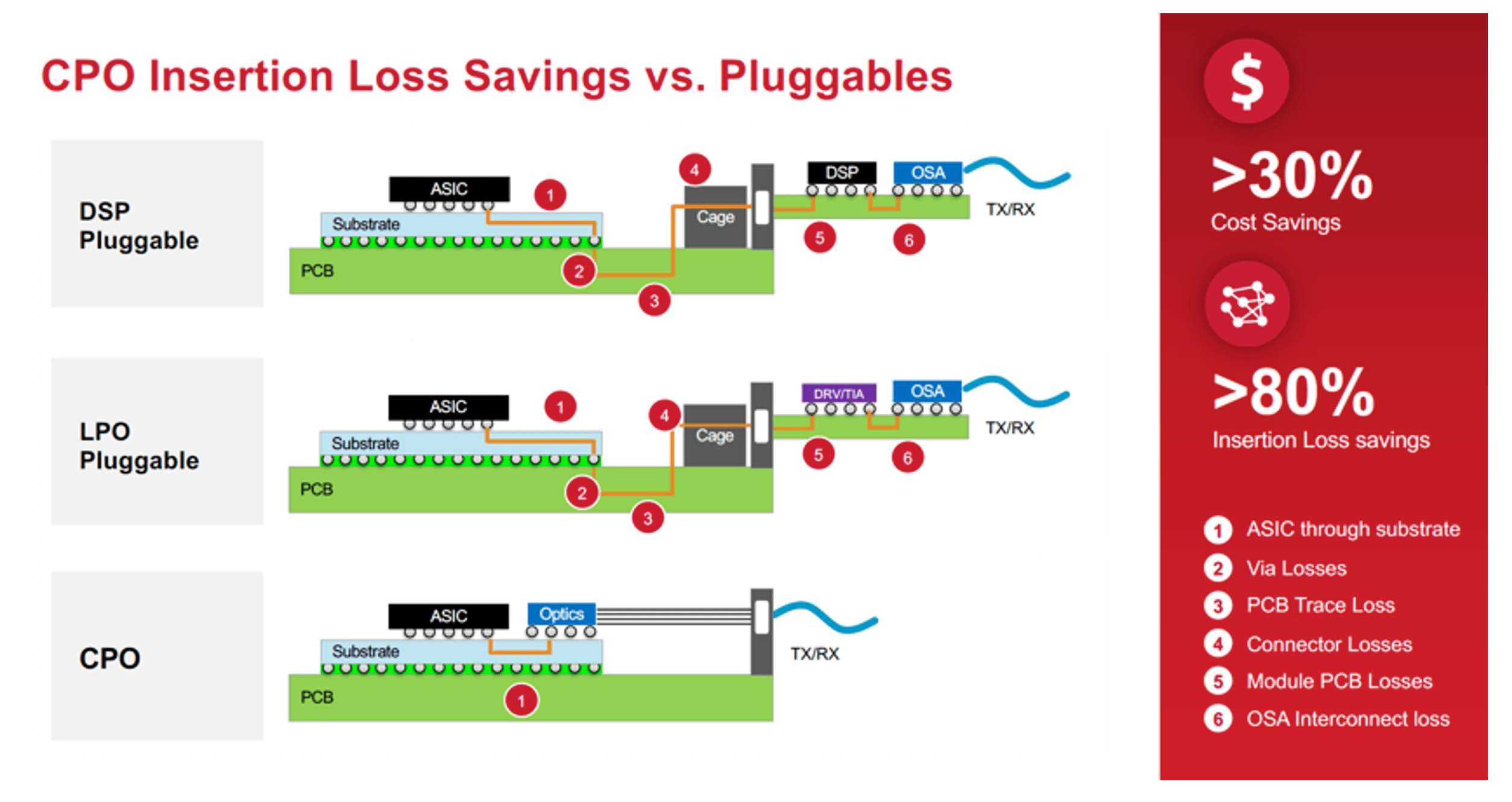
Fig. 1: Co-packaged optics insertion loss savings compared to pluggables. Broadcom sees linear drive pluggable optics as an intermediate step. Source: Broadcom
LPOs are driven directly by the switch SerDes, without re-timers. Re-timers, which extend reach by creating new signals, were once valued for increasing signal, without also amplifying noise — unlike re-drivers, which amplify both. But now, their presence is being questioned because their function increases latency and takes additional power.
“Anything that needs a digital signal processor requires power,” said Rob Shore, senior vice president of marketing at Infinera. “And the number one issue for data center operators, particularly ones trying to build up their artificial intelligence infrastructure, is power. They want to dedicate every watt of power they can to the servers, and as little as possible to the optics.”

Fig. 2 Interfaces without re-timers. Source: Synopsys
To the proponents, LPOs are a well-thought-out compromise between functionality and familiarity. “When it comes to CPOs, there are some understandable questions about reliability if you’re switching from the traditional pluggables to a technology that looks very different in terms of implementation,” said Ansys’s Alam. “LPOs would still have the same form factor as the current pluggables. That’s a big motivation for people to go that route, instead of going CPO, which is going to be radically different.”
Nevertheless, LPOs have their own limitations. “You cannot transmit the data over very long distances,” Alam explained. “The reach is much shorter than CPO. CPO would also offer you more power benefits down the road. Conversely, LPO would offer superior maintainability owing to its modular structure. Ultimately, some groups will go with LPO, some with CPO, and some with both. There are situations where pluggables make sense, such as current pluggable transceivers and LPO, and situations where CPO makes sense. Both will continue to exist and the market share will divide between the two.”
From a design point of view, the challenges for CPO and LPO have a good overlap and should mostly be supported by current EDA tools, especially so for LPO due to its resemblances to current pluggable transceivers. “You can use the same solutions currently getting used in pluggable transceiver designs for LPO, while for CPO there are multiphysics workflows in place to address the emerging packaging challenges,” Alam noted.
Thermal issues
For all the power reduction promises of CPOs, the design is challenged by thermal issues. But it’s not the lasers that are to blame.
“If you’re concerned with thermal issues, the very word ‘laser’ sounds scary,” said Alam. “But with co-packaged optics and on-chip and off-chip lasers, most of the players have their optical engine and the laser on separate chips. Then they take the laser and bring it into the CPO package. The advantages of keeping the laser separate is that you’re contributing less heat to your switching system. In addition, the laser is sensitive to temperature variations, so when you bring that into a 3D-IC, you need to think about the reliability of the laser as well, because of thermal crosstalk and so on. It’s therefore a simpler solution to keep the lasers off-chip. That said, there are already some solutions that have lasers integrated into the CPO package. The bottom line is that whether you have on-chip or off-chip lasers, you need to perform thermal simulations of your entire CPO package to minimize thermal crosstalk, optimize system cooling, and reduce operating temperature to ensure performance and reliability.”
Heat is a big issue in photonics in a way that doesn’t exist in electrical ICs, because it can affect the signal integrity. Nevertheless, while the behavior of some components can be very sensitive to temperature change, circuits usually have feedback loops that adjust the voltage on the thermal tuners and thereby adjust the device temperatures and performance. However, there are some elements that are sensitive to temperature variations that don’t have thermal tuning capabilities.
“You have to be very cognizant of the heat and how that’s impacting your designs,” said Ansys’ Goldman. “We’re moving more to photonics in data centers because copper heats up and glass does not, and light also carries a lot more signals. You can do a lot bigger bandwidth, and it’s at the speed of light. It’s better, faster, cheaper.”
Put simply, it’s not the lasers creating additional heat. It’s the structure of the packaging.
“The challenge for the industry is that you have to co-package this,” said Shukla. “You have to model the performance with the co-packaged deployment. Everybody is trying their best to solve this problem. The photonic die providers, photonic foundries are coming up with these processes so that the thermal dissipation for their photonic components, laser modulators, will be limited. The EDA companies are coming up with flows that will allow the system designers to model this temperature profile so that the performance of optical components can be modeled correctly. For instance, if laser performance changes with an increase in temperature, we need tools that will model that effectively, and something can be done on the digital side to compensate for this degradation in performance. That’s what EDA tools and designers are doing from their side of the puzzle, and the SerDes designers are reducing power from the electrical side.”
However, unlike electronics, in some photonics circuits carefully controlled heat is used to tune lasers, which changes wavelengths as heat increases. But that quality can make thermal overload an even more concerning issue.
“A lot of the structures will have built-in heaters to regulate the resonances and filtering capabilities of their waveguides,” said Chris Mueth, business development, marketing, and technical specialist at Keysight. “It needs to have a feedback loop. If you’re going to have something tuned to a particular wavelength, you need to have control over that. When you start integrating inside of 3D-ICs and you get self-heating of those chips, it just compounds the problem.”
The situation is complicated, but it’s not hopeless. “You need to think about the control loops to handle that. It’s not something that can’t be managed,” said Mueth. “It’s another of the many multi-discipline characteristics that you’ve got to deal with when you’re integrating 3D-ICs and photonics and all these different technologies with physics-based effects.”
Conclusion
After decades of PowerPoint presentations, the once-separate worlds of photonics and electronics appear to be converging.
“Whether it is co-packaged optics, or pluggables, or monolithic integration, photonics is coming closer to electronics in wide-ranging applications, including data center optics and HPC,” said Jigesh Patel, principal, product marketing, EDA group at Synopsys. “This trend requires a paradigm shift in the design innovation — moving from SoC to a system-of-chips approach, where co-design and co-optimization of multiple technologies in a common electronic-photonic design automation environment is a key to commercial success.”
Related Reading
Re-timers Replacing Re-drivers As Signal Speeds Increase
Redrivers are running out of steam as more devices are connected over high-speed protocols.
New Standards Push Co-Packaged Optics
Speed, density, distance, and heat all need to be considered; pluggables still have a future
- SEO Powered Content & PR Distribution. Get Amplified Today.
- PlatoData.Network Vertical Generative Ai. Empower Yourself. Access Here.
- PlatoAiStream. Web3 Intelligence. Knowledge Amplified. Access Here.
- PlatoESG. Carbon, CleanTech, Energy, Environment, Solar, Waste Management. Access Here.
- PlatoHealth. Biotech and Clinical Trials Intelligence. Access Here.
- Source: https://semiengineering.com/linear-drive-optics-may-reduce-data-latency/
- :has
- :is
- :not
- :where
- $UP
- 1
- 2%
- 2023
- 2024
- 2026
- 800
- a
- About
- across
- actual
- add
- addition
- Additional
- address
- adjust
- Adjusted
- ADvantage
- advantages
- affect
- ago
- AI/ML
- All
- allow
- alongside
- already
- also
- amounts
- amplify
- amplifying
- an
- and
- Another
- any
- appear
- applicable
- applications
- approach
- approved
- architects
- architecture
- ARE
- AREA
- argument
- artificial
- artificial intelligence
- AS
- asic
- asked
- At
- attention
- Automation
- b
- ball
- Bandwidth
- BE
- because
- become
- been
- behavior
- being
- benefits
- BEST
- Better
- between
- Big
- bigger
- Bit
- board
- both
- Bottom
- bring
- Broadcom
- broadly
- budget
- build
- buildings
- built-in
- business
- business development
- but
- by
- CAN
- cannot
- capabilities
- carefully
- Center
- Centers
- ceo
- chain
- challenge
- challenged
- challenges
- challenging
- chan
- change
- Changes
- characteristics
- cheaper
- chip
- Chips
- choices
- Chris
- circuits
- closer
- cognizant
- combined
- comes
- coming
- commercial
- Common
- Communication
- Companies
- compared
- compensate
- complicated
- component
- components
- compromise
- computation
- concerned
- concerning
- connected
- Connections
- considerations
- considered
- continue
- continues
- contributing
- control
- controlled
- converging
- conversely
- Conversion
- conversions
- Copper
- correctly
- Costs
- could
- Creating
- Cross
- Crystal
- CTO
- Current
- Currently
- data
- Data Center
- data centers
- deal
- debate
- decade
- decades
- dedicate
- dedicated
- deeper
- demanding
- demands
- density
- deployment
- Design
- designed
- designers
- designs
- developed
- Development
- device
- Devices
- Die
- different
- digital
- directly
- Director
- distance
- distributed
- divide
- do
- does
- Doesn’t
- doing
- done
- Dont
- down
- drive
- driven
- drives
- driving
- due
- Edge
- effectively
- effects
- efficient
- efficiently
- Electronic
- Electronics
- elements
- eliminate
- eliminating
- emerged
- emerging
- Engine
- engineer
- Engineering
- enhance
- enough
- ensure
- Entire
- Environment
- error
- especially
- essential
- Even
- Every
- everybody
- evolve
- evolved
- exist
- expanded
- explained
- extend
- facilitates
- factor
- familiar
- Familiarity
- far
- faster
- February
- feedback
- Fig
- filtering
- First
- Flows
- Focus
- For
- Force
- form
- from
- front
- fully
- function
- functionality
- generated
- geographically
- get
- getting
- glass
- Go
- going
- goldman
- good
- got
- GPUs
- Group
- Group’s
- Growing
- Growth
- handle
- Have
- High
- his
- hopes
- How
- However
- hpc
- HTTPS
- huang
- ICS
- idea
- IEEE
- if
- impacting
- implementation
- in
- Including
- Increase
- Increases
- increasing
- industry
- Infrastructure
- Innovation
- inside
- instance
- instead
- integrated
- Integrating
- integration
- integrity
- Intelligence
- interconnects
- interfaces
- Intermediate
- into
- IP
- issue
- issues
- IT
- ITS
- itself
- Jensen Huang
- just
- Keep
- keeping
- Key
- laser
- lasers
- Latency
- lead
- left
- Legacy
- less
- Level
- light
- like
- limitations
- Limited
- Line
- linear
- little
- Long
- long time
- looking
- LOOKS
- loops
- loss
- Lot
- lower
- maintainability
- major
- make
- MAKES
- managed
- manager
- many
- Market
- market share
- Marketing
- massive
- max-width
- May..
- means
- minimize
- model
- modular
- Monolithic
- more
- most
- mostly
- Motivation
- move
- moving
- much
- multiple
- Need
- needs
- network
- networks
- Nevertheless
- New
- newer
- Noise
- noted
- now
- number
- of
- offer
- on
- once
- ONE
- ones
- operating
- Operations
- operators
- optical
- Optical components
- optics
- optimal
- Optimize
- Option
- or
- Other
- out
- over
- overlap
- own
- package
- packaging
- panel
- paradigm
- particular
- particularly
- partnerships
- past
- path
- paths
- People
- perform
- performance
- Place
- planned
- plato
- Plato Data Intelligence
- PlatoData
- players
- Point
- Point of View
- possible
- power
- Predictions
- presence
- Presentations
- presented
- president
- Principal
- Problem
- processes
- Processor
- Product
- product manager
- Profile
- promises
- Promoted
- properly
- proponents
- protocols
- providers
- publicly
- Push
- puzzle
- quality
- Questioned
- Questions
- quite
- R&D
- radically
- rapidly
- rather
- reach
- ready
- really
- recently
- reduce
- Reduced
- reducing
- reduction
- Regulate
- reliability
- removes
- removing
- rendering
- requires
- result
- reverse
- Rich
- rightful
- road
- rob
- root
- Route
- Run
- running
- Said
- same
- Save
- Savings
- see
- sees
- senior
- sense
- sensitive
- separate
- Servers
- several
- Share
- shift
- shorter
- should
- side
- Signal
- signals
- simpler
- simplicity
- simplified
- simply
- simulations
- single
- situation
- situations
- slow
- So
- so Far
- solution
- Solutions
- SOLVE
- Solving
- some
- something
- sounds
- Source
- specialist
- speed
- speeds
- spread
- Squeeze
- standalone
- standard
- standards
- start
- Starting
- Steam
- Step
- Still
- Strategic
- Strategic Partnerships
- structure
- structures
- substrate
- success
- such
- superior
- Supported
- Surface
- Switch
- system
- Systems
- tailored
- Take
- takes
- taking
- talked
- talking
- Task
- task force
- teams
- Technical
- Technologies
- Technology
- terms
- than
- that
- The
- their
- themselves
- then
- There.
- thereby
- therefore
- thermal
- These
- they
- things
- Think
- this
- those
- Through
- time
- to
- together
- Tony
- tools
- traditional
- Train
- Training
- transition
- transmission
- transmit
- Trend
- trying
- tune
- tuned
- tuning
- two
- Ultimately
- understandable
- unit
- unlike
- unsustainable
- us
- use
- used
- using
- usually
- value
- valued
- variants
- variations
- Versus
- very
- via
- vice
- Vice President
- View
- Voltage
- Wall
- want
- was
- wavelengths
- Way..
- ways
- we
- WELL
- well-known
- were
- What
- when
- whether
- which
- while
- WHO
- why
- will
- with
- without
- Word
- Work
- workflows
- working
- world’s
- would
- you
- Your
- youtube
- zephyrnet