The technology to enable sampling and the need for more metrology and inspection data in a production setting have aligned just in time to address the semiconductor industry’s newest and most complex manufacturing processes.
In both wafer and assembly manufacturing, engineering teams have long relied on imaging tools to measure critical features and to inspect for defects after specific processes. These tools, which utilize different emitter sources — optical, X-ray, and e-beam — are essential for process development, yield ramp, and production monitoring.
Optical systems continue to be the primary workhorse systems in a production setting. They have the highest throughput, and for decades their measurement resolution has kept pace with the critical dimensions and defect sizes of interest. But optical is running out of steam at ≤14nm advanced CMOS logic nodes, and during assembly with bump/pillar pitches ≤50µm.
At the same time, the need to ferret out subtle defects is increasing. Advanced CMOS design and process complexity result in smaller features with higher design layout sensitivity. Likewise, advanced packaging processes, such as 2.5D, utilize higher interconnect density, which in turn necessitates co-planarity of over a million bumps/pillars. The imaging challenges come from the significantly higher ratio of scanned area to required measurement resolution. For a 300mm wafer, the ratio is on order of 109:1 and for a 50 x 50mm packaging substrate the ratio is on order of 104:1. The imaging challenges increase when you add in the throughput requirements to support a 100% sampling rate in a manufacturing production scenario.
Fortunately, due to engineering ingenuity, and advances in computation and CCD detectors, the equipment makers have created systems that meet this seemingly daunting challenge. This includes equipment that identifies defects and measures critical dimensions, which is essential for process development, yield ramp, and excursion control. In addition, there have been improvements in equipment setup, and close to real-time process control.
Still, results will vary depending on sampling rates during process development and production, which is a tradeoff of time/money vs yield/reliability that is determined by factory management.
“Inspection is not just for yield learning,” said Indranil De, general and engineering manager of e-beam tools at PDF Solutions. “Even in a production manufacturing flow, a fab has to decide in advance how to spread out its inspection budget. Inspection does not just happen at transistor, metal-1 and metal-2 levels. Fabs are doing inspections at every metal layer. They’re all being inspected at different rates. Factory teams spread out their investment dollars in a manner they think is most efficient with respect to likely excursion points.”
There is a common assumption that earlier data is better, which increases the demand for more imaging-derived data. But it needs to be the right data at a useful point in time for engineers to take action. And in a manufacturing setting, it can’t cost too much time or money. CMOS wafers already take at least three months to fabricate, while advanced packaging takes at least one month.
So ROI needs to include a realistic assessment of the associated risks of not detecting failures in the end customer’s system. That, in turn, depends on how and where a chip will be used. For example, escapes to the field have a heightened risk for mission- and safety-critical systems, particularly those found in data centers, automotive, and military/aerospace applications. In these scenarios, 100% inspection and metrology becomes a justified insurance policy.
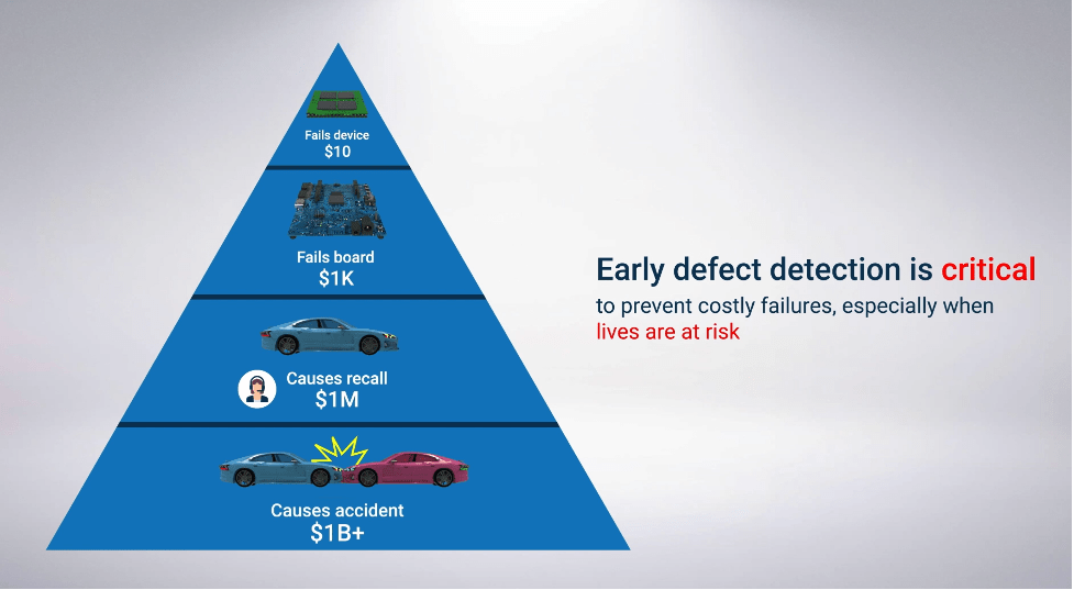
Fig. 1: Increasing risk and associated cost with later failure detection. Source: Bruker
Nevertheless, engineering managers still may need convincing, because 100% inspection/metrology is expensive. “There are some quality considerations, but at the end of the day somebody has to make money from it,” explained Frank Chen, director of applications and product management at Bruker. “So how do you explain the commercial aspect to show the value of adopting 100% inspection?”
Chen provided a hypothetical return-on-investment (ROI) calculation for adopting 100% inspection for CPU advanced packaging with Bruker’s X200 X-ray inspection system. (See figure 2.)
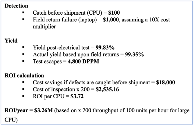
Fig. 2: Cost of field failure vs. failure before shipment, based on 4,156 units. Source: Bruker
Raising the bar
Combining high throughput with high resolution creates a demanding set of specifications for imaging systems. Throughput to support 100% sampling raises the bar even higher.
To meet this challenge, engineering teams must leverage advances in detectors, adopting different emitter sources, and build effective computational methods. Part of what makes this possible is the narrowness in the measurement objective. The more specific it is, the more effective, economical, and efficient an imaging system can be designed for it.
Imaging modalities include optical, X-ray and e-beam, each choosing from specific detection schemes. But the basic components remain the same — a movement system, an ‘illumination’ source, an image acquisition, an optional multi-objective design to adjust magnification, and the computational resources to analyze the data using detection and measurement algorithms.
Put simply, it all comes down to speed. “Two things drive your speed,” said John Hoffman, computer vision engineering manager at Nordson Test & Inspection. “How fast can you move from one site to the next? That’s a function of your motion system, and it depends upon how heavy is the sensor/wafer that is being moved, how much stability you need to have, and how fast you have to stop. Then there’s the data acquisition portion. How many images do you need to take? How much light? How fast is your camera? How many different lighting schemes do you need? My team’s mandate is to develop all the signal processing algorithms. They have to be faster than the move time and the data acquisition combined. We want the bottleneck to be a physical limit, not a computational limit.”
Physical limits come from the realities of the movement system, the physics of the chosen imaging method, and the desired field of view (FOV) and measurement resolution. The former is the area for the projected light/X-ray/e-beam. The number of pixels in the detector provides the square area that each pixel covers, and the A/D conversion gives the number of data bits that convert detection brightness to a digital code.
Systems can be continuous-scan or stop-and-move. For optical, continuous scan has been the standard.
“Optical image-based inspection technology is mainstream in HVM environments for both the front-end and back-end facilities, as it can reach high sampling rates to fulfill the need of 100% inspection for certain process control steps,” said Nathan Peng, product marketing manager, Onto Innovation. “Continuous scan is preferred to reach full wafer/panel sampling 100% inspection. The time rate really depends on the resolution or defect size, but typically for 300mm wafers the throughput can be up to 100 wafers per hour (WPH) if the pixel resolution is in 10µm range.”
The rapid increase in pixel density in CCD cameras has enabled much faster throughput times and higher resolution. Hoffman noted that Nordson’s first 3D sensor used a 5-megapixel camera, and 8 years later its 3D sensors used an 85-megapixel camera, which represents a 20-fold data increase. With this increase in data, stop-and-move systems can compete with continuous scan systems on speed and outperform them in resolution. Imaging methods like fringe projection profilometry can readily take advantage of this and other hardware technology improvements. [1,2]
“For optical you have a very limited flexibility with a scan-on-the-fly phase profilometry system to achieve the accuracy levels that our customers want,” Hoffman said. “We’re finding we can get significantly better accuracy and repeatability if we do move-and-stop. We’re using digital light projectors, which have a ton of flexibility in them. They’ll allow us to fine-tune the image collection process to maximize the amount of information we’re extracting with each image. We minimize the number of collected images and we maximize utility to speed up data acquisition. In our systems we use multiple digital light projectors and multiple cameras. This enables us to project light from one projector and simultaneously collect images from multiple cameras.”
In creating imaging systems, engineers need to consider field of view (area per image), pixel resolution (area per pixel) and data quantization (number of bits per pixel) as they trade off speed with resolution. For advanced packaging applications, these tradeoffs are evident when comparing X-ray systems.
“In a conventional failure analysis X-ray system, you’re looking at a few millimeter by millimeter fields of view to get that high resolution for a 1 micron feature size,” said Bruker’s Chen. “That’s an order of magnitude difference of 103. A scan can take about 15 minutes for a fast system, or many hours for a slow system. As you study the needs for advanced packaging, you actually need a magnitude difference of 105. High-throughput tools can have a very large field of view, but sacrifice on the resolution. But that’s not going to be applicable for many advanced packaging applications. The resolution is too poor. That’s the gap that we fill.”

Fig. 3: Comparison of different X-ray systems with respect to wafers per hour, field of view (FOV), and resolution per pixel. Source: Bruker
With the ability to measure in the 1nm range, e-beam inspection would be ideal to comprehend tiny defects in the most advanced CMOS logic and memory process nodes. A typical e-beam inspection system uses a raster scan method. To understand its measurement time constraints, one needs to comprehend the physics.
“An e-beam column has a specific spot width with a specified current which represents the number of electrons striking the area during the measurement time. Smaller current translates to longer measurement time per pixel (as defined by the spot width),” explained PDF’s De. “Consider a 10 x 10µm square broken up into 10 x 10nm pixels. Each e-beam measurement equals 100ns. With 1 million 10nm pixels to measure, the time becomes about 0.1 sec.”
State of the art e-beam systems (single/multi-column) perform a raster scan of a few hundred square millimeters per hour. Extrapolating a 300mm full wafer scan would require about 237 hours. Therefore, e-beam tools have historically been relegated to R&D and failure analysis lab use.
The key is knowing what areas to look at more closely. “The ability to look at very specific locations gives you a huge throughput advantage,” De said. “You change from a raster-scan approach to a point-scan approach because you jump from one location to another location.”
Advantages of 100% inspection
With these new imaging systems, which offer faster throughput and higher resolution, chipmakers can consider 100% sampling rates in places it has never been an option.
When engineers focus on the defects that matter, inspection systems can be narrowed to that defect type, and then cost-effectively support 100% sampling. For example, say there’s more interest in edge and backside wafer inspection.
“When a customer moves to a more advanced node, they increase quality control during manufacturing, including extending from frontside inspection of the wafer to the edge and backside of the wafer,” said Onto’s Peng. “With our edge and backside inspection module we can see chipping and cracks at the wafer edge or a backside scratch. These may propagate or transfer to die area and can eventually cause yield loss. The trend we see is customers adopting 100% edge/backside inspection for their wafers during QA.”
Another scenario involves buried defects. For decades, salicide cracks on first metal interconnect and partial voids in contacts/vias have plagued yield and failure analysis. Their subsequent electrical impact can manifest as timing delays, which cause system failures. Finding them earlier in the wafer processing supports process improvements and detection of bad die prior to wafer test.
E-beam imaging with voltage contrast has shown success in identifying such defects, but as discussed earlier, the measurement time per pixel during a raster scan doesn’t lend itself to a production environment. However, pruning down the locations to look at enables a point scan method, which increases the throughput.
Using a street traffic analogy, PDF’s De explained the tradeoffs between e-beam spot size, current and measurement locations as follows, “You can have a certain width of a street and can travel at a certain speed. Now you can make your street larger or you can travel faster. But you’re still limited by how many electrons you can pump per unit time. Instead of looking at every location on that street (i.e. pixel), you could look at only the locations of interest and scan 2% of the street. Now you can travel faster on that on that street.”
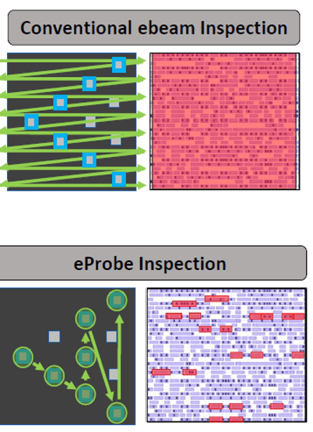
Fig. 4: Comparison between a raster-scan method (above) with a point-scan method (below). Source: PDF Solutions
Using this approach in a two-to-four hour period, PDFs e-beam system can scan several billion selected features on a 300mm wafer. In a production environment, a manufacturer can judiciously elect to perform such scans. But the pre-work to define the locations of interest, which includes a highly detailed design sensitivity analysis, is crucial for this type of inspection. The analysis combines layout sensitivity at each layer, and detailed signal and power interconnect routing information. For example, an engineer may care about a routing with only 3 redundant vias, and not care about any with 10 redundant vias.
Inspection and metrology in 2.5D packaging
With high-performance computing devices fueling 2.5D packaging, the bond density of die(s) and substrate has skyrocketed. Product functionality and reliability now depend on close to a million bonded solder bumps or copper pillars, which are decreasing in size/pitch to 25µm for Cu pillars and soon 10 µm for Cu pads.
This spurs the need for a 100% inspection and metrology during the formation of bumps/pillars and post-bond metallurgical integrity. The co-planarity of millions of bumps/pillars affects warpage and bonding. As a result, the outcome metrics of specific processes which impact co-planarity are especially important to assembly process engineers.
One flow for copper pillar formation is similar to inter-metal via formation. There is electroplating into a hole masked by photoresist. After deposition, the photoresist is removed and then underbump metalization is deposited, followed by a reflow step to form the solder cap.
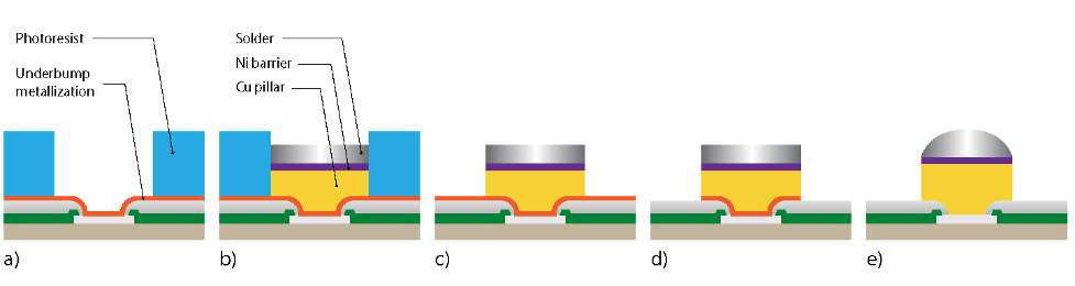
Fig. 5: Copper pillar bump process flow. Conventional bump height measurement is done after photoresist stripping; a) before bumping; b) bump plating; c) photoresist strip; d) UBM etching; e) solder reflow. Source: Nordson Test & Inspection
In a multi-step process flow engineering teams have a vested interest in metrology from the middle of the process as opposed to the end.
“I would have naively assumed a customer going through that process would just want to do a final inspection of the copper pillars,” said Nordson’s Hoffman. “Are these copper pillars good or not? But it turns out that what they want is to inspect (measure) before they do the photoresist strip. This is an in-situ measurement in the middle of the 10 to 12 manufacturing processing steps. They’re interested in the photoresist thickness because that drives how high these pillars get, and simultaneously measuring the pillar height.”
Optical methods have challenges due to reflections from shiny surfaces and interference between reflections from the multiple layers. To make such measurements on Cu and photoresist structures using a fringe profilometry methodology requires sophisticated signal processing algorithms to sort out all the reflections and merging of multiple images.
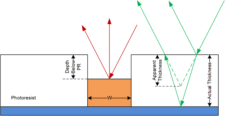
Fig. 6: Measurement of bump height before photoresist stripping, using light refracted through the photoresist to determine the photoresist thickness and calculate bump height above the wafer surface. Source: Nordson Test & Inspection
Production-capable post-bond quality has been limited to optical inspection at the edge. An X-ray system, in contrast, can ‘see’ the bond. And with appropriate area per pixel resolution, it can assess the bond quality for the typical defect mechanisms like solder necking, head-in-pillow, and partial cracks. But it’s not just pixel area resolution that matters. The quantization of each pixel’s signal affects image interpretability.

Fig. 7: Difference between 8 and 16 bits of dynamic range when measuring a metal structure. Source: Bruker
Increasing the dynamic range from 8 to 16 bits enables more accurate defect identification and more precise bump height measurement. The ability to measure bump height after bonding provides information to assess die-to-substrate warpage.
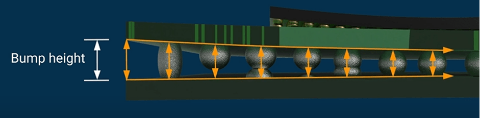
Fig. 8: X-ray system’s assessment of bump height after bond. Source Bruker
Conclusion
Successfully managing advanced CMOS and 2.5D assembly processes requires increased inspection and metrology data. In some scenarios, 100% sampling has huge benefits to product yield and reliability. However, changing existing manufacturing flows has an activation energy to overcome, which is higher when adding a new inspection or metrology tool. The cost is ever-present in decision-makers’ minds.
“We optimize things so that we maximize our speed, because at the end of the day that’s what customers want,” said Nordson’s Hoffman. “If you can double the throughput, you can half their costs to get to 100% sampling.”
References
[1] https://en.wikipedia.org/wiki/Structured-light_3D_scanner
[2] S. Feng, et al., “Calibration of fringe projection profilometry: a comparative review,” Optics and Lasers in Engineering 143, 106622, 2021. https://doi.org/10.1016/j.optlaseng.2021.106622
Related Reading
Bump Co-Planarity And Inconsistencies Cause Yield, Reliability Issues
Advanced packaging challenges grow as chips and package sizes shrink; different equipment, technologies gain traction.
Auto Chipmakers Dig Down To 10ppb
Driving to 10 defective parts-per-billion quality is all about finding, predicting nuanced behavior in ICs.
E-Beam’s Role Grows For Detecting IC Defects
Basic applications and new approaches combine to speed up semiconductor inspection.
- SEO Powered Content & PR Distribution. Get Amplified Today.
- PlatoData.Network Vertical Generative Ai. Empower Yourself. Access Here.
- PlatoAiStream. Web3 Intelligence. Knowledge Amplified. Access Here.
- PlatoESG. Carbon, CleanTech, Energy, Environment, Solar, Waste Management. Access Here.
- PlatoHealth. Biotech and Clinical Trials Intelligence. Access Here.
- Source: https://semiengineering.com/progress-in-wafer-and-package-level-defect-inspection/
- :has
- :is
- :not
- :where
- $UP
- 1
- 10
- 100
- 12
- 15%
- 16
- 2%
- 2021
- 237
- 3d
- 4
- 5
- 50
- 6
- 7
- 8
- a
- ability
- About
- above
- accuracy
- accurate
- Achieve
- acquisition
- Action
- Activation
- actually
- add
- adding
- addition
- address
- adjust
- Adopting
- advance
- advanced
- advances
- ADvantage
- affects
- After
- AL
- algorithms
- aligned
- All
- allow
- already
- amount
- an
- analysis
- analyze
- and
- Another
- any
- applicable
- applications
- approach
- approaches
- appropriate
- ARE
- AREA
- areas
- Art
- AS
- aspect
- Assembly
- assess
- assessment
- associated
- assumed
- assumption
- At
- automotive
- b
- Back-end
- Bad
- bar
- based
- basic
- BE
- because
- becomes
- been
- before
- behavior
- being
- below
- benefits
- Better
- between
- Billion
- bits
- bond
- bonded
- both
- bottleneck
- Broken
- budget
- build
- but
- by
- calculate
- calculation
- camera
- cameras
- CAN
- Can Get
- cap
- care
- Cause
- CCD
- Centers
- certain
- challenge
- challenges
- change
- changing
- chen
- chip
- Chips
- choosing
- chosen
- Close
- closely
- code
- collect
- collected
- collection
- Column
- combine
- combined
- combines
- come
- comes
- commercial
- Common
- comparing
- comparison
- compete
- complex
- complexity
- components
- comprehend
- computation
- computational
- computer
- Computer Vision
- computing
- Consider
- considerations
- constraints
- continue
- continuous
- contrast
- control
- conventional
- Conversion
- convert
- convincing
- Copper
- Cost
- Costs
- could
- covers
- CPU
- created
- creates
- Creating
- critical
- crucial
- Current
- customer
- Customers
- data
- data centers
- day
- de
- decades
- decide
- decreasing
- defect
- define
- defined
- delays
- Demand
- demanding
- density
- depend
- Depending
- depends
- deposited
- Design
- designed
- desired
- detailed
- detecting
- Detection
- Determine
- determined
- develop
- Development
- Devices
- Die
- difference
- different
- DIG
- digital
- dimensions
- Director
- discussed
- do
- does
- Doesn’t
- doing
- dollars
- done
- double
- down
- drive
- drives
- due
- during
- dynamic
- e
- E&T
- each
- Earlier
- Edge
- Effective
- efficient
- electrons
- enable
- enabled
- enables
- end
- energy
- engineer
- Engineering
- Engineers
- Environment
- environments
- Equals
- equipment
- especially
- essential
- Ether (ETH)
- Even
- eventually
- Every
- evident
- example
- existing
- expensive
- Explain
- explained
- extending
- facilities
- factory
- Failure
- failures
- FAST
- faster
- Feature
- Features
- few
- field
- Fields
- Fig
- Figure
- fill
- final
- finding
- First
- first 3D
- Flexibility
- flow
- Flows
- Focus
- followed
- follows
- For
- for yield
- form
- formation
- Former
- found
- frank
- from
- fueling
- Fulfill
- full
- function
- functionality
- Gain
- gap
- General
- get
- gives
- going
- good
- Grow
- Grows
- Half
- happen
- Hardware
- Have
- heavy
- height
- heightened
- High
- high-performance
- higher
- highest
- highly
- historically
- Hole
- hour
- HOURS
- How
- How High
- How To
- However
- HTTPS
- huge
- hundred
- i
- ICS
- ideal
- Identification
- identifies
- identifying
- if
- image
- images
- Imaging
- Impact
- important
- improvements
- in
- include
- includes
- Including
- inconsistencies
- Increase
- increased
- Increases
- increasing
- industry’s
- information
- ingenuity
- instead
- insurance
- integrity
- interest
- interested
- interference
- into
- investment
- involves
- IT
- ITS
- itself
- John
- jump
- just
- justified
- kept
- Key
- Knowing
- lab
- large
- larger
- lasers
- later
- layer
- layers
- Layout
- learning
- least
- LEND
- Level
- levels
- Leverage
- light
- Lighting
- like
- likely
- likewise
- LIMIT
- Limited
- limits
- location
- locations
- logic
- Long
- longer
- Look
- looking
- loss
- magnitude
- Mainstream
- make
- make money
- Makers
- MAKES
- management
- manager
- Managers
- managing
- mandate
- manner
- Manufacturer
- manufacturing
- many
- Marketing
- Matter
- Matters
- max-width
- Maximize
- May..
- measure
- measurement
- measurements
- measures
- measuring
- mechanisms
- Meet
- Memory
- merging
- metal
- method
- Methodology
- methods
- Metrics
- Metrology
- micron
- Middle
- million
- millions
- minds
- minimize
- minutes
- modalities
- module
- money
- monitoring
- Month
- months
- more
- most
- motion
- move
- moved
- movement
- moves
- much
- multiple
- must
- my
- nathan
- necessitates
- Need
- needs
- never
- New
- Newest
- next
- node
- nodes
- noted
- now
- nuanced
- number
- objective
- of
- off
- offer
- on
- ONE
- only
- opposed
- optical
- optics
- Optimize
- Option
- or
- order
- Other
- our
- out
- Outcome
- Outperform
- over
- Overcome
- Pace
- package
- packaging
- part
- partial
- particularly
- per
- perform
- period
- phase
- physical
- Physics
- Pillar
- pillars
- pitches
- Pixel
- Places
- plagued
- plato
- Plato Data Intelligence
- PlatoData
- Point
- points
- policy
- poor
- portion
- possible
- power
- precise
- predicting
- preferred
- primary
- Prior
- process
- processes
- processing
- Product
- product management
- Production
- Progress
- project
- projected
- Projection
- provided
- provides
- pump
- Q&A
- quality
- R&D
- raises
- Ramp
- range
- rapid
- Rate
- Rates
- ratio
- reach
- readily
- real-time
- realistic
- realities
- really
- redundant
- Reflections
- reliability
- remain
- Removed
- represents
- require
- required
- Requirements
- requires
- Resolution
- Resources
- respect
- result
- Results
- review
- right
- Risk
- risks
- ROI
- Role
- routing
- running
- s
- sacrifice
- Said
- same
- say
- scan
- scans
- scenario
- scenarios
- schemes
- scratch
- SEC
- see
- seemingly
- selected
- semiconductor
- Sensitivity
- sensors
- set
- setting
- setup
- several
- show
- shown
- Signal
- significantly
- similar
- simply
- simultaneously
- site
- Size
- sizes
- slow
- smaller
- So
- Solutions
- some
- Soon
- sophisticated
- sort
- Source
- Sources
- specific
- specifications
- specified
- speed
- Spot
- spread
- square
- Stability
- standard
- Steam
- Step
- Steps
- Still
- Stop
- street
- Strip
- stripping
- structure
- structures
- Study
- subsequent
- substrate
- subtle
- success
- such
- support
- Supports
- Surface
- system
- Systems
- Take
- takes
- teams
- Technologies
- Technology
- test
- than
- that
- The
- The Area
- their
- Them
- then
- There.
- therefore
- These
- they
- things
- Think
- this
- those
- three
- Through
- throughput
- time
- times
- timing
- tiny
- to
- Ton
- too
- tool
- tools
- traction
- trade
- tradeoff
- tradeoffs
- traffic
- transfer
- travel
- Trend
- TURN
- turns
- type
- typical
- typically
- understand
- unit
- units
- upon
- us
- use
- used
- useful
- uses
- using
- utility
- utilize
- value
- vary
- very
- via
- View
- vision
- Voltage
- vs
- want
- we
- What
- when
- which
- while
- Wikipedia
- will
- with
- would
- X
- x-ray
- years
- Yield
- you
- Your
- zephyrnet