
[This post is authored by SpicyIP intern Pranav Aggarwal. Pranav is a second-year student pursuing B.A.LL.B.(Hons) at Rajiv Gandhi National University of Law, Punjab. He has a keen interest in commercial laws, especially in IP and allied fields. His previous post can be accessed here.]
Some journals have a practice of providing research prompts on which people can potentially write. But I realised that sometimes prompts without a choice can work really well too. Swaraj shared a Youtube link and asked me to work on it. It had semi-conductors and Prof. Paulraj (both of which I had no iota of information on, prior to this assignment).
Professor Arogyaswami Paulraj, an Indian American academician and engineer, is currently a Professor Emeritus in the Department of Electrical Engineering at Stanford University. He has 80 patents to his credit, among which his invention of the Multiple Input Multiple Output (MIMO) has been phenomenal in the world of wireless networking systems. He was invited to IIC for a session on the Global Perspective on Semiconductors, which can be accessed here.
He gave a fantastic and very informative presentation on this area, which I’d highly recommend, explaining the larger role of the US and China in the global semiconductor market.The presentation ended with a slide from where my search began. The heading of the last slide said ‘Key to Success is Innovation and IP’. Intellectual Property and Semiconductors? Armed with my recently gained knowledge from the presentation and the many questions that popped up while listening to it, I wanted to look a bit more at this question. So, in this post, we will have an overview of the existing IP protections for semiconductors. Along with that, we will further explore where India stands in this discourse and what lies ahead for her.
Semiconductors & Integrated Circuits Designs
Looking at the list of IP legislations in India, perhaps the most under-discussed one is the Semiconductor Integrated Circuits Layout Design Act, 2000 (SICLDA) (in line with TRIPS obligations). The necessity for such an Act arose because one could not protect Integrated Circuit (IC) layout design under the existing IP rights. The design right, generally, denied protection to primarily functional designs and taking a patent for an IC layout was not possible for the reason that most conventional patent systems didn’t allow protection to topography or layout of an IC. However, it hasn’t been able to attract much application for the limited protection it provides. Only three registrations have been done thus far; details of which can be seen in the Annual IP Report 2021-22 (Page 85).
Internationally, the Washington Treaty on Intellectual Property in Respect of Integrated Circuits was adopted in 1989 to introduce separate protection for IC layout designs. Although India is a signatory to the treaty, this Treaty never came into force. So, the question arises, if not here, then where are the global companies like Intel and Qualcomm locating their IP rights?
The Patents Tale: From 1960s till Now
Prof Paulraj’s presentation answers this question: Patents, or more specifically, 5,77,000 Patents globally (past and present) (see also). Although IC layout design cannot be protected under patents, the novel features and innovative manufacturing processes of these chips is patentable.It was patents that American and Chinese countries have been using since the 1960s to protect innovation in semiconductors ICs or ‘chips’, as they are generally called. Initially, during the 1960s and 70s, the patent rights, both product and process, were concentrated in small units that handled everything from designing to manufacturing of the silicon slabs and chips. But outsourcing standardised processes and improvement in cost and production efficiency required division of these processes into fab and fabless. The actual manufacturing of the silicon slabs and the chips was done in fab units (short for “fabrication”), such as Taiwan SemiConductor Manufacturers (TSM); while the fabless units would just focus on the designing and the sale of the chips (for example, Qualcomm). As the division happened, it also divided the Patents rights between the fab (process patents) and fabless (product patents) units.
As the processes became more and more complex because of continuous innovation in the sector, the need for further division was felt. Hence, from the 1990s, the third division also emerged which was the Integrated Device Manufacturing (IDM) which carried out the assembly and the required testing (for example, Amkor). The innovations in the IDM further lead to another set of patents being registered. Interestingly enough, during this period, companies which were only the outsourced manufacturing arm of the huge fabless companies, also began their own chip designing and distribution. Although the whole semiconductor production cut across various regions, currently, no single country can achieve self-reliance because ultimately, only a handful of companies dominate this industry across all these regional units.
Mr. India, No Watch Please !!
In 1987, an Anil Kapoor starrer, Mr. India got huge traction for the special cloaking device which made the protagonist invisible when worn. The developing India, I believe, never shed that cloaking device when it comes to semiconductors. Till now, India’s demand for semiconductors has been majorly met by imports. A major reason for the same has been related to the limited natural reserves of Silicon, a primary semiconductor, that India has in comparison to China and US as seen in the table below.
| Region (2022) | Silicon Reserve (in metric tonnes) |
| Total | 8,800,000 |
| China | 6,000,000 |
| US | 310,000 |
| India | 59,000 |
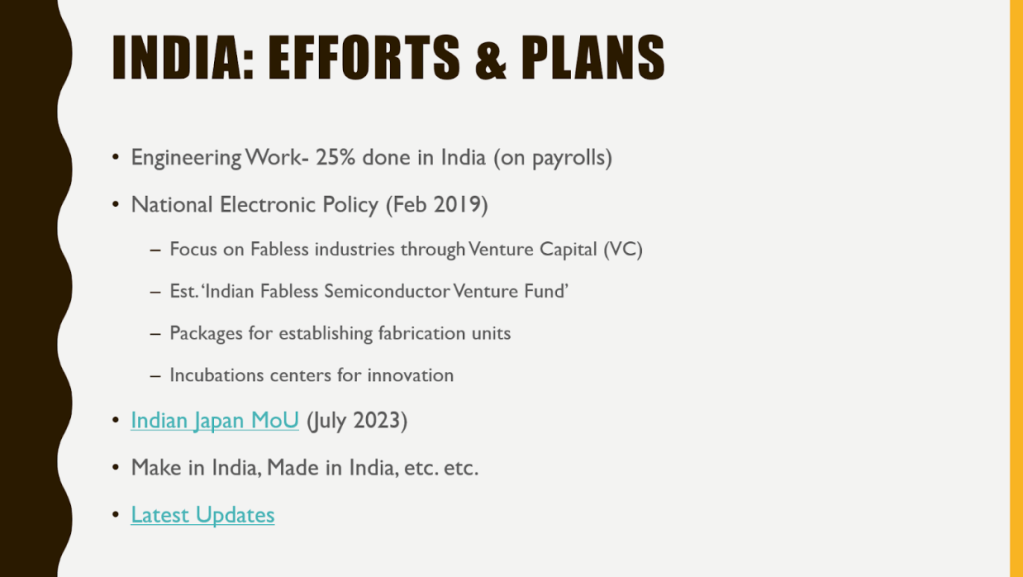
However, recently, the Indian government has been trying to make a move to reduce this dependency. The National Electronics Policy, 2019 and the Indian Semiconductor Mission (ISM) in 2021 at least show some intent on the part of the government to promote fab, fabless and IDM enterprises in India.
Under the ISM, the government plans a financial outlay of around INR 76,000 crore (USD 9.13 billion approx). However, two things lie unaddressed. First, is this outlay sufficient? Because (as mentioned by Prof. Paulraj in his presentation) around USD 10 Billion is the basic cost to establish a fab unit. Although industry support has been evident, still, will it help the (almost) non-existent industry to meet the Indian demand? Secondly, what concerns me more is that will the government own any IP rights on the innovative products and processes being developed on its stipulated outlay, or will have a say in how they are commercialised?
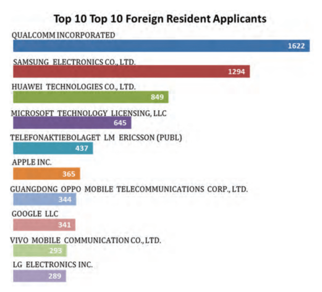
Herein, it becomes important to note that as per the Annual IP report 2021-22, the highest number of foreign applicants has been chip giants like Qualcommn, Samsung, Huawei. A senior executive of Samsung even shared that through its Indian semiconductor research arm, it has around a thousand patents at its credit. Perhaps, through these patents, these companies have been ‘fortifying’ their profits that will come from licensing as soon as Indian companies enter this market.
The Way Forward
After whatever I could gather on semiconductors, the newspaper gave me another thing to think about. ‘China acquires Nvidia chips despite US ban’. The news was just a para short but it made me realise that now, semiconductors have become such a big deal that even the whole geo-politics is not untouched by it. And the reason for the same is simple, Economics. 20 Billion Devices, overall impact of USD 7 Trillion, USD 500 Billion in revenue, USD 2 trillion investment in the next decade and the list goes on and on.
No country would like to leave this because leaving this would not just mean huge trade deficits but a back seat to the digital revolution. Not a bit of it can be imagined without microprocessors, the ‘nano-accelerators’ of the digital economy. And India being no exception to this has to find this way through it. Preferably, as Prof. Paulraj also advised, the fabless sector can take a major lead in India due to its lower capital requirements compared to fab units. Additionally, alternatives to Silicon have to be searched for to decrease our dependence on others for it. Graphene (discussed a decade ago on the blog here), for instance, can be a good alternative considering the recent developments as seen in Georgia Institute of Technology. Even in India, both process and product patents have been granted in relation to graphene. For instance, IIT Roorkee got a process patent for the synthesis of graphene oxide. Anyhow, we should come out with more such innovations, which will be undoubtedly more challenging but will hold much better prospects for the future economy of the country. I hope this piece, atleast, will be a food for thought for the discussions and developments to come.
Thanks again to Prof Paulraj for the IIC presentation, and to Swaraj for the inputs and the prompt!
Referenced Readings:
- SEO Powered Content & PR Distribution. Get Amplified Today.
- PlatoData.Network Vertical Generative Ai. Empower Yourself. Access Here.
- PlatoAiStream. Web3 Intelligence. Knowledge Amplified. Access Here.
- PlatoESG. Carbon, CleanTech, Energy, Environment, Solar, Waste Management. Access Here.
- PlatoHealth. Biotech and Clinical Trials Intelligence. Access Here.
- Source: https://spicyip.com/2024/02/semiconductors-ip-india-a-road-less-travelled.html
- :has
- :is
- :not
- :where
- $UP
- 000
- 02
- 05
- 1
- 10
- 13
- 2%
- 20
- 2019
- 2021
- 2023
- 4
- 5
- 500
- 6
- 7
- 77
- 8
- 80
- 800
- 9
- a
- Able
- About
- accessed
- Achieve
- Acquires
- across
- Act
- actual
- Additionally
- adopted
- advised
- again
- Aggarwal
- ago
- ahead
- All
- allow
- almost
- along
- also
- alternative
- alternatives
- Although
- American
- among
- an
- and
- annual
- Another
- answers
- any
- Apple
- APPLE INC
- applicants
- Application
- applications
- ARE
- AREA
- ARM
- armed
- around
- AS
- asked
- Assembly
- assignment
- At
- attract
- authored
- b
- back
- basic
- BE
- became
- because
- become
- becomes
- been
- began
- being
- believe
- below
- Better
- between
- Big
- Billion
- Bit
- Blog
- both
- but
- by
- called
- came
- CAN
- cannot
- capital
- capital requirements
- carried
- Centers
- challenging
- China
- chinese
- chip
- Chips
- choice
- circuit
- circuits
- Cms
- CO
- come
- comes
- commercial
- Communication
- Companies
- compared
- comparison
- complex
- Concentrated
- Concerns
- considering
- continuous
- conventional
- Corp
- Cost
- could
- countries
- country
- credit
- Currently
- Cut
- deal
- decade
- decrease
- Demand
- denied
- Department
- dependence
- Dependency
- Design
- designing
- designs
- Despite
- details
- developed
- developing
- developments
- device
- Devices
- digital
- Digital economy
- digital revolution
- discourse
- discussed
- discussions
- distribution
- divided
- Division
- dominate
- done
- due
- during
- economy
- efforts
- electrical engineering
- Electronic
- Electronics
- emerged
- ended
- engineer
- Engineering
- enough
- Enter
- enterprises
- Ericsson
- especially
- establish
- establishing
- etc
- Ether (ETH)
- Even
- everything
- evident
- example
- exception
- executive
- existing
- explaining
- explore
- fantastic
- far
- Features
- Feb
- felt
- Fields
- financial
- Find
- First
- Focus
- following
- food
- Food for thought
- For
- Force
- foreign
- from
- functional
- further
- future
- gained
- gather
- gave
- generally
- giants
- Global
- Globally
- Goes
- good
- got
- Government
- granted
- Graphene
- Guangdong
- had
- handful
- handled
- happened
- Have
- he
- Heading
- help
- hence
- her
- here
- highest
- highly
- his
- hold
- hope
- How
- However
- HTML
- HTTPS
- Huawei
- huge
- i
- ICS
- if
- imagined
- Impact
- important
- imports
- improvement
- in
- Inc.
- india
- Indian
- indian government
- industries
- industry
- information
- informative
- Innovation
- innovations
- innovative
- input
- inputs
- instance
- Institute
- integrated
- Intel
- intellectual
- intellectual property
- intent
- interest
- internal
- into
- introduce
- Invention
- investment
- invisible
- invited
- IOTA
- IP
- IT
- ITS
- Japan
- July
- just
- Kapoor
- Keen
- knowledge
- larger
- Last
- latest
- Latest Updates
- Law
- Laws
- Layout
- lead
- least
- Leave
- leaving
- less
- LG
- LG Electronics
- Licensing
- lie
- lies
- like
- Limited
- Line
- LINK
- List
- Listening
- ll
- LLC
- locating
- Look
- lower
- Ltd
- made
- major
- make
- Manufacturers
- manufacturing
- many
- Market
- max-width
- me
- mean
- Meet
- mentioned
- met
- metric
- Microsoft
- Mission
- Mobile
- more
- most
- MOU
- move
- much
- multiple
- my
- National
- Natural
- necessity
- Need
- networking
- never
- next
- no
- note
- novel
- now
- number
- Nvidia
- obligations
- of
- on
- ONE
- only
- oppo
- or
- Others
- our
- out
- output
- Outsourcing
- overall
- overview
- own
- packages
- page
- PARA
- part
- past
- patent
- Patents
- Payrolls
- People
- per
- perhaps
- period
- perspective
- phenomenal
- piece
- plans
- plato
- Plato Data Intelligence
- PlatoData
- please
- policy
- possible
- Post
- potentially
- practice
- present
- presentation
- previous
- primarily
- primary
- Prior
- process
- processes
- Product
- Production
- Products
- prof
- Professor
- profits
- promote
- prompts
- property
- prospects
- protagonist
- protect
- protected
- protection
- provides
- providing
- pursuing
- qualcomm
- question
- Questions
- really
- reason
- recent
- recently
- recommend
- reduce
- regional
- regions
- registered
- related
- relation
- report
- required
- Requirements
- research
- reserves
- respect
- revenue
- Revolution
- right
- rights
- road
- Role
- Said
- sale
- same
- Samsung
- say
- Search
- sector
- see
- seen
- semiconductor
- Semiconductors
- senior
- separate
- session
- set
- shared
- shed
- Short
- should
- show
- signatory
- Silicon
- Simple
- since
- single
- Slide
- small
- So
- some
- sometimes
- Soon
- special
- specifically
- stands
- stanford
- Stanford university
- Still
- Student
- success
- such
- sufficient
- synthesis
- Systems
- table
- Taiwan
- Take
- taking
- tale
- Technologies
- Technology
- telecommunications
- Testing
- text
- that
- The
- The Future
- the world
- their
- then
- These
- they
- thing
- things
- Think
- Third
- this
- thought
- thousand
- three
- Through
- Thus
- till
- to
- too
- top
- Top 10
- traction
- trade
- Trillion
- trying
- two
- Ultimately
- under
- undoubtedly
- unit
- units
- university
- untouched
- Updates
- us
- USD
- using
- various
- VC
- venture
- venture capital
- venture capital (VC)
- very
- vivo
- wanted
- was
- washington
- Watch
- Way..
- we
- WELL
- were
- What
- whatever
- when
- which
- while
- whole
- Wikipedia
- will
- wireless
- with
- without
- Work
- world
- would
- write
- youtube
- zephyrnet


![Webinar on “How Patent Monopolies on Biologics and Vaccines Work” [November 22]](https://platoaistream.net/wp-content/uploads/2023/11/webinar-on-how-patent-monopolies-on-biologics-and-vaccines-work-november-22-360x509.jpg)