News: Suppliers
5 September 2023
Shin-Etsu Chemical Co Ltd of Tokyo, Japan has announced the market launch of QST (Qromis Substrate Technology) — a composite material substrate licensed in 2019 exclusively from Qromis Inc of Santa Clara, CA, USA — for the growth of gallium nitride (GaN) power devices.
Since QST substrate is designed to have the same coefficient of thermal expansion (CTE) as GaN, it enables suppression of warpage and cracking of the GaN epitaxial layer and can hence enable large-diameter, high-quality thick GaN epitaxial growth. It is hence expected to be applied to power devices and RF devices (5G and beyond 5G), which have been growing rapidly in recent years, as well as to micro-LED growth for micro-LED displays.
In addition to selling QST substrates, Shin-Etsu Chemical will also sell GaN grown QST substrates upon customer request. The firm currently has a line-up of 6”- and 8”-diameter substrates, and it is working on 12”-diameter substrates. Since 2021, for each respective application for power devices, RF devices and LEDs, sample evaluation and device development has been progressing with numerous customers in Japan and globally. Especially for power devices, continuous evaluation is underway for devices in the wide range of 650-1800V.
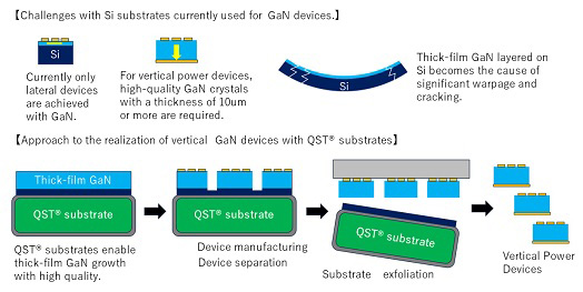
Shin-Etsu Chemical says that it has progressively made many improvements to QST substrates. An example is the significant reduction in defect density originating from the bonding process, enabling the supply of high-quality QST substrates. In addition, for the thicker GaN films that many customers have requested, the firm has promoted the provision of template substrates with optimized buffer layers, enabling customers to realize stable epitaxial growth of more than 10μm thickness. Furthermore, various results have been reported, including thick-film GaN growth exceeding 20μm using QST substrates and the achievement of 1800V breakdown voltage in power devices.
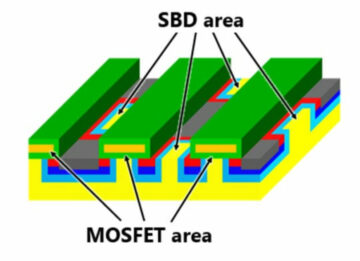
Moreover, Shin-Etsu Chemical and Oki Electric Industry Co Ltd have jointly developed technology for exfoliating GaN from QST substrates and bonding it to substrates made of different materials using Oki’s Crystal Film Bonding (CFB) technology. Up to now, most GaN power devices have been lateral devices, but CFB technology takes advantage of the characteristics of QST substrates to realize vertical power devices that can control large currents by exfoliating a thick layer of high-quality GaN from an insulating QST substrate. For customers that are manufacturing GaN devices, Shin-Etsu Chemical will provide QST substrates or GaN grown QST substrates and Oki Electric Industry will provide its CFB technology through partnering or licensing. The two firms hence hope to contribute to the advancement of vertical power devices.
Shin-Etsu Chemical is giving a presentation on progress in QST product development at SEMICON Taiwan 2023 in Taipei (6–8 September).
Shin-Etsu licenses Qromis’ GaN substrate technology
- SEO Powered Content & PR Distribution. Get Amplified Today.
- PlatoData.Network Vertical Generative Ai. Empower Yourself. Access Here.
- PlatoAiStream. Web3 Intelligence. Knowledge Amplified. Access Here.
- PlatoESG. Automotive / EVs, Carbon, CleanTech, Energy, Environment, Solar, Waste Management. Access Here.
- PlatoHealth. Biotech and Clinical Trials Intelligence. Access Here.
- ChartPrime. Elevate your Trading Game with ChartPrime. Access Here.
- BlockOffsets. Modernizing Environmental Offset Ownership. Access Here.
- Source: https://www.semiconductor-today.com/news_items/2023/sep/shinetsu-050923.shtml
- :has
- :is
- $UP
- 2019
- 2021
- 2023
- 5G
- a
- achievement
- addition
- advancement
- ADvantage
- also
- an
- and
- announced
- Application
- applied
- ARE
- AS
- At
- BE
- been
- Beyond
- Breakdown
- buffer
- but
- by
- CA
- CAN
- characteristics
- chemical
- Clara
- CO
- continuous
- contribute
- control
- Crystal
- Currently
- customer
- Customers
- density
- designed
- developed
- Development
- device
- Devices
- different
- displays
- each
- Electric
- enable
- enables
- enabling
- especially
- evaluation
- example
- exclusively
- expansion
- expected
- Film
- films
- Firm
- firms
- For
- from
- Furthermore
- Giving
- Globally
- Growing
- grown
- Growth
- Have
- hence
- high-quality
- hope
- http
- HTTPS
- improvements
- in
- Including
- industry
- IT
- items
- ITS
- Japan
- jpg
- large
- launch
- launches
- layer
- layers
- Licensed
- licenses
- Licensing
- Ltd
- made
- manufacturing
- many
- Market
- material
- materials
- more
- most
- now
- numerous
- of
- on
- optimized
- or
- originating
- partnering
- plato
- Plato Data Intelligence
- PlatoData
- power
- presentation
- process
- Product
- Progress
- progressing
- progressively
- Promoted
- provide
- provision
- range
- rapidly
- realize
- recent
- reduction
- related
- Reported
- request
- requested
- respective
- Results
- same
- Santa
- says
- sell
- Selling
- September
- significant
- since
- stable
- supply
- suppression
- Taiwan
- takes
- Technology
- template
- than
- that
- The
- thermal
- Through
- to
- tokyo
- two
- Underway
- upon
- USA
- using
- various
- vertical
- Voltage
- WELL
- which
- wide
- Wide range
- will
- with
- working
- years
- zephyrnet