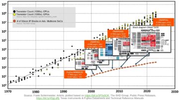
Circuit scaling is starting to hit a wall as the laws of physics clash with exponential increases in the volume of data, forcing chipmakers to take a much closer look at silicon photonics as a way of moving data from where it is collected to where it is processed and stored.
The laws of physics are immutable. Put simply, there are limits to how fast an electron can travel through copper. The speed of an electron, while fast on a macroscopic scale, encounters significant resistance as pathways shrink, leading to heat generation and power inefficiencies. In contrast, silicon photonics circumvents these electrical limitations by harnessing the swiftness of photons, which travel at the speed of light and are not bound by the resistive properties of materials like copper. Unlike electrons, photons do not generate significant heat, can carry more data due to their higher frequency, and suffer from less signal degradation.
“Companies are reaching limitations in terms of how much bandwidth they can carry through the substrates,” says Yin Chang, senior vice president of sales and marketing for ASE. “If you’re not able to meet those requirements, then photonics is the only option.”
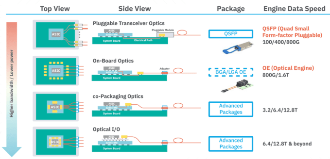
Fig. 1: Photonics harnesses the speed of light for faster data transmission. Source ASE.
Silicon photonics has seized a pivotal role in data centers, where high-bandwidth and energy-efficient data transmission are paramount. As AI, cloud computing, and IoT devices proliferate, the need for efficient data handling intensifies. Photonic ICs (PICs), in this context, help perpetuate operations that demand higher data transport rates with reduced power demand. These innovations point to an increasingly bright future for silicon photonics in scenarios requiring swift, voluminous data communication.
“The usage of optics due to growth of AI clusters is growing significantly,” says Manish Mehta, vice president of marketing and operations for optical systems at Broadcom. “The architecture is effectively optical from the API server to the aggregation switch.”
The global market for silicon photonics was valued at $1.26 billion in 2022, with an expected CAGR of 25.7% by 2030, with an expected market value of $7.86 billion, according to a report by Vantage Market Research.
Apart from data centers, silicon photonics is trailblazing developments in other areas, such as lidar in automobiles, which along with cameras and radar is considered essential for object detection. It also is revolutionizing optical projection technology for advanced imaging systems, augmented reality (AR) displays, and ultra-high-definition holographic projections.
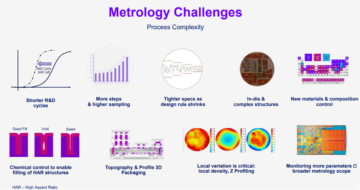
But despite significant advancements and potential market opportunities, existing manufacturing processes are limiting the scalability and mass production of silicon photonics components. Manufacturing is often manual and labor-intensive due to the intricacy and precision required in fabricating optical components.
Manufacturing processes
Silicon photonics incorporates the optical functionalities of PICs — such as light generation, modulation, and detection — on a silicon substrate, enabling optical and electronic devices to coexist on the same integrated circuit chip.
In silicon photonic devices, a laser is controlled and manipulated in ways similar to electronic signals in traditional ICs. Silicon’s high refractive index contrast allows tight confinement and miniaturized components, which makes it possible to create complex optical circuits in small footprints. A key advantage of silicon photonics is it can be fabricated using standard CMOS manufacturing technology, allowing for cost-effective mass production using existing manufacturing equipment and materials in conventional fab lines.
Nonetheless, integration is not so simple. “Integrating light onto a chip creates a challenge,” says Vik Chaudhry, senior director of product marketing and business development at Amkor. “You have to generate a laser, and you have to have optical alignment, and that’s a totally different beast for manufacturing.”
The manufacturing process begins with imaging and etching passive optical devices, such as waveguides and couplers, which guide and direct the light on the chip. Devices like modulators convert electronic signals into optical ones by changing the intensity or phase of light passing through them. At the receiving end, photodetectors convert the optical signals back into electronic ones, completing the communication loop.
Creating waveguides demands more sophisticated patterns and features than those in standard electronic circuits. One of the challenges of using photons as data carriers is their predilection to travel in a straight line. The rectilinear shapes of traditional photolithography can lead to sub-optimal performance when light transmits through waveguide bends, potentially causing scattering and signal loss, especially in tight turns.
This is where curvilinear masks fit into the picture. They allow for the creation of smoother, more rounded corners and complex shapes that more closely mimic the desired path of light within the photonic circuit. This results in waveguides with more gradual curves, which in turn can significantly reduce optical losses and improve device performance. The improved accuracy and control over waveguide shapes made possible by curvilinear masks enable the design of more efficient and compact photonic components, which is particularly important as photonic circuits become more complex and denser.
It is also possible to cross waveguides without creating a short because photons don’t interact the way electrons do. Two electrons in the same channel will repel each other, but with photons, it’s possible to multiplex signals on the same circuit using a multiplexer (mux) and demultiplexer (demux).
For PICs, silicon-on-insulator (SOI) wafers are preferred over conventional silicon wafers. SOI wafers are particularly advantageous because they include a thin silicon layer on top for crafting waveguides, with an insulating buried oxide layer beneath that keeps optical signals pristine by minimizing loss to the substrate.

Fig. 2: Cross-sectional structure of channel-type Si wire waveguide. Source: Semiconductor Engineering.
Once the patterns are set, the next stage involves material deposition. The silicon found in traditional electronic fabrication lacks certain key properties needed for effective optical transmission. The heart of the issue is silicon’s indirect bandgap property, which hinders its ability to “lase,” or emit light efficiently. This inherent characteristic of silicon necessitates the deposition of supplementary materials that boast a direct bandgap, such as those from the III-V semiconductor family like gallium arsenide, widely used for lasers and LEDs in optical systems.
This indirect bandgap also accounts for silicon’s sub-optimal light detection performance.
Materials like germanium supplement silicon in the photodetector due to their more effective direct bandgap nature at telecommunications wavelengths. Silicon also falls short in its nonlinear optical qualities, which are crucial for advanced functionalities such as optical switching and wavelength conversion, requiring complementary materials with stronger nonlinear responses.
Additionally, silicon’s high thermal optical coefficient means that any temperature change significantly alters its refractive index, leading to a wavelength drift in photonic applications unless carefully managed. For the optical transparency vital for telecommunication frequencies, silicon nitride is used.
The doping of silicon must be handled with finesse — imperative for the formation of p-n junctions that modulate the light traveling through these PICs. Unlike the doping for electronic purposes, which aims to control the flow of electrons, with PICs the focus is how silicon interacts with photons. That dictates the efficiency and clarity of the light signal modulation. This often necessitates direct bonding of III-V semiconductor materials onto the silicon wafer, ensuring that the sources and the detectors are properly integrated within the PIC.
“A challenge for silicon photonics is adding these techniques in a high-volume environment,” adds Chaudhry. “You have to have processes, which you can do repeatedly at volumes of millions per week. Today, silicon photonics is still a very manual process. We need to figure out how to do optical connects in an automated manner before we can think about bringing it to high volume manufacturing.”
The packaging problem
The steep demands of high-performance packaging further complicate the transition to photonics. Unlike traditional electrical components, photonic components require precise alignment to maintain signal integrity, often using active alignment techniques, which are more time-consuming and costly. This drive for high-performance packaging has ramped up the complexity of assembly, leaving manufacturers facing difficult questions on how to scale these operations cost-effectively.
“We can see co-packaged optics on the horizon, and people are asking how to incorporate silicon photonics,” adds Chaudhry. “It is a challenge connecting optics to the die and then connecting multiple dies together.”
There’s also a matter of thermal management. Photonics circuits are highly sensitive to temperature changes, necessitating sophisticated cooling solutions that do not interfere with optical transmission. That adds yet another layer of complexity to the packaging process.
“These materials are typically pretty poor from a CTE perspective,” says David Fromm, COO and vice president of engineering at Promex Industries. “Because they have lower transition temperatures, you can easily reach a point where the CTE is much larger than the other things around them that you’re dealing with, and the materials themselves are not typically optimized for CTE. They’re optimized for optics. So that creates a lot of problems.”
Packaging and assembly are typically a fraction of the cost compared to electronic circuits, but the complexity of integrating PICs flips that ratio. Some research estimates the cost of packaging, assembly, and test for photonics devices is as much as 80% of the total module cost. [1]
“There’s a lot of interest in photonics recently, especially in co-packaged optics,” adds ASE’s Chang. “We are working on many different processes for on-package photonics to dramatically increase the bandwidth of the data transfer. The goal is to create better performance and higher efficiency.”
Each optical element — from waveguides to modulators and photodetectors — must be encapsulated in a way that protects its function, while also enabling it to interact seamlessly with its electronic counterparts. Moreover, the packaging must support the stabilization of photonic structures, minimizing any displacement or vibration that could disrupt optical signal integrity.
Both electronic and optical testing are also critical to guarantee the integrity of the signal paths and the performance of each optical element on the chip. This includes scrutinizing the waveguides for any potential optical losses, evaluating modulators and detectors for efficiency, and thoroughly assessing the overall data transmission capabilities.
Latest developments
Despite the challenges, there are advances. One such breakthrough is the development of ultra-low-loss waveguides. The problem has been figuring out a way to streamline light through the chip with minimal signal degradation. That is now becoming achievable with new materials and refined fabrication techniques.
Engineers are exploring both old and new materials to improve light efficiency and control on silicon substrates. This includes silicon nitride (Si3N4), which has been in use for 50 years, and Hydex, a family of photonic glass materials characterized by their high index of refraction and ultra-low optical losses in the near-infrared range, making them especially effective for use in telecommunications. Hydex can be carefully tailored during the manufacturing process for specific opto-mechanical properties that increase the integration density and functionality of photonic components.
Hydex glass is produced through a specialized sol-gel process, which involves the transition of a solution into a solid gel phase. From there, it is processed further to create glass. By adjusting the conditions and the composition of the precursor solution, manufacturers can modify the glass’s final properties, such as its thermo-optic coefficient or its index contrast with respect to the cladding material.
Photonic engineers also are developing waveguides that can handle multiple modes and polarizations of light within the same structure. This means that these circuits can carry more information without needing to increase in physical size.
Additionally, they are integrating length-multiplexing features, which greatly boost the data throughput of photonic integrated circuits (PICs). By incorporating elements for wavelength division multiplexing directly onto the chip, multiple wavelengths of light can be used simultaneously, allowing for parallel data streams—similar to opening up multiple lanes on a highway for faster traffic flow.
Moreover, the design of photonic circuits is currently undergoing an overhaul. Chip designs now include complex routing systems and optical resonators, such as micro-ring resonators and arrayed waveguide gratings, which can sort and direct information at the speed of light.
However, with this increased complexity comes the need for PICs to adapt to the thermal sensitivity of photonic components. Innovations like on-chip temperature control systems, such as thermal tuners and localized cooling, are being developed to ensure that PICs can maintain consistent performance despite changes in their operating environment.
Conclusion
Photonics devices already have established a crucial role within data centers, facilitating high-speed and energy-efficient communication between densely packed server racks and interconnected storage units. But the potential applications for silicon photonics extend far beyond data centers.
Lidar, for example, relies on laser pulses to measure distances and generate precise 3D maps of environments. Silicon photonics can enhance lidar systems by enabling compact and cost-effective solutions for automotive safety systems, autonomous vehicles, and environmental monitoring.
Silicon photonics also is poised to revolutionize image projection technology. By leveraging its ability to manipulate light with precision, silicon photonics can enable the development of miniature, high-resolution projectors for applications ranging from mobile devices to augmented reality headsets.
Still, the opportunities for research and advancement in silicon photonics are limited by the number of foundries with the capacity to produce them. Open-access foundries, which allow a variety of business customers to use their manufacturing facilities, are pivotal for smaller companies and research institutions that do not have the resources to build in-house production lines. This bottleneck stifles innovation and slows the pace at which new photonic designs can be tested and brought to market. The scarcity of such facilities can delay prototyping and increase costs for small-scale producers, potentially stifling the diversity and proliferation of photonics solutions.
Moreover, the specific requirements of silicon photonics, such as the need to integrate both electronic and photonic components with nanoscale precision, means that only a few foundries have the capabilities to manufacture these chips. For silicon photonics to reach its potential, investment in the expansion of these open-access foundries is imperative to provide more industry players with the ability to innovate and bring products to the market.
- Latkowski et al., “Open Standards for Automation of Testing of Photonic Integrated Circuits,” 2019. IEEE Journal of Selected Topics in Quantum Electronics. Vol. 25 (5).
Related Reading
Photonics: The Former And Future Solution
Twenty-five years ago, photonics was supposed to be the future of high technology. Has that future finally arrived?
Photonics: Harnessing The Power Of Light
Opinion: The evolution of photonics engineering will encompass novel materials and cutting-edge techniques.
- SEO Powered Content & PR Distribution. Get Amplified Today.
- PlatoData.Network Vertical Generative Ai. Empower Yourself. Access Here.
- PlatoAiStream. Web3 Intelligence. Knowledge Amplified. Access Here.
- PlatoESG. Carbon, CleanTech, Energy, Environment, Solar, Waste Management. Access Here.
- PlatoHealth. Biotech and Clinical Trials Intelligence. Access Here.
- Source: https://semiengineering.com/silicon-photonics-manufacturing-ramps-up/
- :has
- :is
- :not
- :where
- $UP
- 05
- 1
- 2%
- 2019
- 2022
- 2030
- 25
- 26
- 3d
- 5
- 50
- 50 Years
- a
- ability
- Able
- About
- According
- Accounts
- accuracy
- achievable
- active
- adapt
- adding
- Adds
- adjusting
- advanced
- advancement
- advancements
- advances
- ADvantage
- advantageous
- aggregation
- ago
- AI
- aims
- AL
- alignment
- allow
- Allowing
- allows
- along
- already
- also
- an
- and
- Another
- any
- api
- applications
- AR
- architecture
- ARE
- areas
- around
- arrived
- AS
- asking
- Assembly
- Assessing
- At
- augmented
- Augmented Reality
- augmented reality (ar)
- Automated
- Automation
- automobiles
- automotive
- autonomous
- autonomous vehicles
- back
- Bandwidth
- BE
- because
- become
- becoming
- been
- before
- begins
- being
- Better
- between
- Beyond
- Billion
- boost
- both
- bottleneck
- bound
- breakthrough
- Bright
- bring
- Bringing
- Broadcom
- brought
- build
- business
- business customers
- business development
- but
- by
- CAGR
- cameras
- CAN
- capabilities
- Capacity
- carefully
- carriers
- carry
- causing
- Centers
- certain
- challenge
- challenges
- chang
- change
- Changes
- changing
- Channel
- characteristic
- characterized
- chip
- Chips
- circuit
- circuits
- clarity
- Clash
- closely
- closer
- Cloud
- cloud computing
- coexist
- collected
- comes
- Communication
- compact
- Companies
- compared
- complementary
- completing
- complex
- complexity
- components
- composition
- computing
- conditions
- Connecting
- connects
- considered
- consistent
- context
- contrast
- control
- controlled
- conventional
- Conversion
- convert
- coo
- Copper
- corners
- Cost
- cost-effective
- costly
- Costs
- could
- counterparts
- crafting
- create
- creates
- Creating
- creation
- critical
- Cross
- crucial
- Currently
- curves
- Customers
- cutting-edge
- data
- data centers
- David
- dealing
- delay
- Demand
- demands
- density
- Design
- designs
- desired
- Despite
- Detection
- developed
- developing
- Development
- developments
- device
- Devices
- dictates
- Die
- different
- difficult
- direct
- directly
- Director
- displacement
- displays
- Disrupt
- Diversity
- Division
- do
- Dont
- dramatically
- drive
- due
- during
- E&T
- each
- easily
- Effective
- effectively
- efficiency
- efficient
- efficiently
- Electronic
- Electronics
- electrons
- element
- elements
- enable
- enabling
- encapsulated
- encompass
- end
- Engineering
- Engineers
- enhance
- ensure
- ensuring
- Environment
- environmental
- environments
- equipment
- especially
- essential
- established
- estimates
- Ether (ETH)
- evaluating
- evolution
- example
- existing
- expansion
- expected
- Exploring
- exponential
- extend
- fabricating
- facilitating
- facilities
- facing
- Falls
- family
- far
- FAST
- faster
- Features
- few
- Fig
- Figure
- final
- Finally
- Finesse
- fit
- Flips
- flow
- Focus
- For
- forcing
- formation
- Former
- found
- fraction
- Frequency
- from
- function
- functionalities
- functionality
- further
- future
- generate
- generation
- glass
- Global
- global market
- goal
- gradual
- greatly
- Growing
- Growth
- guarantee
- guide
- handle
- handled
- Handling
- harnesses
- Harnessing
- Have
- headsets
- Heart
- help
- High
- high-performance
- high-resolution
- higher
- highly
- Highway
- hinders
- Hit
- holographic
- horizon
- How
- How To
- HTTPS
- ICS
- IEEE
- image
- Imaging
- immutable
- imperative
- important
- improve
- improved
- in
- In other
- include
- includes
- incorporate
- incorporates
- incorporating
- Increase
- increased
- Increases
- increasingly
- index
- industry
- inefficiencies
- information
- inherent
- innovate
- Innovation
- innovations
- institutions
- integrate
- integrated
- Integrating
- integration
- integrity
- Intensifies
- interact
- interacts
- interconnected
- interest
- interfere
- into
- investment
- involves
- iot
- iot devices
- issue
- IT
- ITS
- journal
- Key
- lacks
- larger
- laser
- lasers
- Laws
- layer
- lead
- leading
- leaving
- less
- leveraging
- lidar
- light
- like
- limitations
- Limited
- limiting
- limits
- Line
- lines
- Look
- loss
- losses
- Lot
- lower
- made
- maintain
- MAKES
- Making
- managed
- management
- manipulate
- manipulated
- manner
- manual
- Manufacturers
- manufacturing
- many
- Maps
- Market
- market opportunities
- market value
- Marketing
- Masks
- Mass
- material
- materials
- Matter
- max-width
- means
- measure
- Meet
- millions
- minimal
- minimizing
- Mobile
- mobile devices
- modes
- modify
- module
- monitoring
- more
- more efficient
- Moreover
- moving
- much
- multiple
- must
- Nature
- necessitates
- necessitating
- Need
- needed
- needing
- New
- next
- nonlinear
- novel
- now
- number
- object
- Object Detection
- of
- often
- Old
- on
- ONE
- ones
- only
- onto
- opening
- operating
- Operations
- opportunities
- optical
- Optical components
- optics
- optimized
- Option
- or
- Other
- out
- over
- overall
- Overhaul
- Pace
- packaging
- packed
- Parallel
- Paramount
- particularly
- Passing
- passive
- path
- paths
- pathways
- patterns
- People
- per
- performance
- perpetuate
- perspective
- phase
- Photons
- physical
- Physics
- picture
- pivotal
- plato
- Plato Data Intelligence
- PlatoData
- players
- Point
- poised
- poor
- possible
- potential
- potentially
- power
- precise
- Precision
- precursor
- preferred
- president
- pretty
- Problem
- problems
- process
- processed
- processes
- produce
- Produced
- Producers
- Product
- Production
- Products
- Projection
- projections
- proliferation
- properly
- properties
- property
- protects
- prototyping
- provide
- purposes
- put
- qualities
- Quantum
- Questions
- radar
- Ramps
- range
- ranging
- Rates
- ratio
- reach
- reaching
- Reality
- receiving
- recently
- reduce
- Reduced
- refined
- relies
- REPEATEDLY
- report
- require
- required
- Requirements
- research
- Research Institutions
- Resistance
- Resources
- respect
- responses
- Results
- revolutionize
- Revolutionizing
- Role
- routing
- Safety
- sales
- Sales and Marketing
- same
- says
- Scalability
- Scale
- scaling
- Scarcity
- scenarios
- seamlessly
- see
- seized
- selected
- semiconductor
- senior
- sensitive
- Sensitivity
- server
- set
- shapes
- Short
- Signal
- signals
- significant
- significantly
- Silicon
- similar
- Simple
- simply
- simultaneously
- Size
- slows
- small
- smaller
- smoother
- So
- solid
- solution
- Solutions
- some
- sophisticated
- sort
- Source
- Sources
- specialized
- specific
- speed
- Stage
- standard
- standards
- Starting
- steep
- stifles
- Still
- storage
- stored
- straight
- streamline
- stronger
- structure
- structures
- substrate
- such
- suffer
- supplement
- support
- supposed
- SWIFT
- Switch
- Systems
- tailored
- Take
- techniques
- Technology
- telecommunication
- telecommunications
- terms
- test
- tested
- Testing
- than
- that
- The
- The Future
- their
- Them
- themselves
- then
- There.
- thermal
- These
- they
- thin
- things
- Think
- this
- thoroughly
- those
- Through
- throughput
- time-consuming
- to
- today
- together
- top
- Topics
- Total
- TOTALLY
- traditional
- traffic
- trailblazing
- transfer
- transition
- transmission
- Transparency
- transport
- travel
- Traveling
- TURN
- turns
- two
- typically
- undergoing
- units
- unless
- unlike
- Usage
- use
- used
- using
- value
- valued
- variety
- Vehicles
- very
- vice
- Vice President
- vital
- volume
- volumes
- Wall
- was
- wavelengths
- Way..
- ways
- we
- week
- when
- which
- while
- widely
- will
- Wire
- with
- within
- without
- working
- years
- yet
- you
- zephyrnet