News: Optoelectronics
14 March 2024
Although micro-LEDs exist as single chips and waveguides as fiber-optic cables, the materials required to make them are too heterogenous to integrate these electronics and photonics components onto a single chip. However, a novel etching technique could enable the combining of optoelectronic light sources and photonic fiber optics.
Researchers at Friedrich Schiller University Jena and Technische Universität Braunschweig have launched the joint project OptoGaN (‘Highly integrated microphotonic modules in nitride technologies’) focusing on porous gallium nitride, which has been awarded about €600,000 of funding by the Federal Ministry of Education and Research (BMBF) for a three-year term until October 2026.
The research groups reckon that their technology could serve an array of potential applications. The project partners hope to establish three applications with one start-up each as demonstrators. Their research could benefit technologies such as waveguides, neuromorphic computing and the trapped-ion quantum computer operated by the Quantum Valley Lower Saxony network. Meanwhile, the newly founded Nitride Technology Center (NTC) at TU Braunschweig will support the further development of nitride technology at the highest level and bring it into application.
The technology could be applied through, for example, the process of manipulating the ions of a quantum computer, which still requires large-scale laser systems. If more and more quantum bits are to be incorporated into these computers, then their laser systems must become significantly smaller, ideally no larger than a chip. However, silicon dioxide — the standard material for waveguides on chips — absorbs the critical wavelengths of light. Gallium nitride could provide a solution, as porous GaN has a low index of refraction and facilitates waveguiding of light to individual ions with minimal losses.
Complementary expertise in handling gallium nitride
The porous material is the result of a new, selective etching technique that turns electrically conductive areas into air-filled channels (pores). The corresponding electrical contrast is realized through ion implantation with masks. It is reckoned that this technique could even open the door to three-dimensional waveguides with complex optical light conduction. Also, gallium nitride and the novel process are compatible with the procedure used to manufacture LEDs and laser diodes to date, making it possible to realize integrated electronic and photonic circuits.
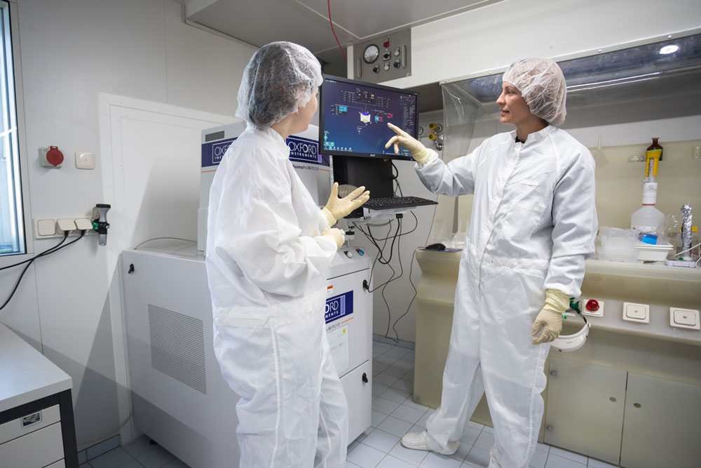
Picture: At TU Braunschweig, scientists etch porous semiconductor crystals made of GaN. (Photo: Max Fuhrmann/TU Braunschweig.)
Researchers at Jena and Braunschweig are combining their complementary expertise and specialist equipment to realize these innovative semiconductor channels for light guiding, since the etching technique has both electronic and chemical components. First, researchers in Braunschweig produce the base material, layer by layer. The material is then shipped to Jena for ion implantation. The researchers in Jena dope the chip and make targeted changes to its electronic properties. Finally, the chip returns to Braunschweig, where there chemical etching process creates the final, porous structure.
- SEO Powered Content & PR Distribution. Get Amplified Today.
- PlatoData.Network Vertical Generative Ai. Empower Yourself. Access Here.
- PlatoAiStream. Web3 Intelligence. Knowledge Amplified. Access Here.
- PlatoESG. Carbon, CleanTech, Energy, Environment, Solar, Waste Management. Access Here.
- PlatoHealth. Biotech and Clinical Trials Intelligence. Access Here.
- Source: https://www.semiconductor-today.com/news_items/2024/mar/optogan-140324.shtml
- :has
- :is
- :where
- 000
- 2026
- a
- About
- absorbs
- also
- an
- and
- Application
- applications
- applied
- ARE
- areas
- Array
- AS
- At
- awarded
- base
- BE
- become
- been
- benefit
- bits
- both
- bring
- by
- cables
- Center
- Changes
- channels
- chemical
- chip
- Chips
- circuits
- collaborating
- combining
- compatible
- complementary
- complex
- components
- computer
- computers
- computing
- contrast
- Corresponding
- could
- creates
- critical
- Date
- Development
- Devices
- Door
- each
- Education
- Electronic
- Electronics
- enable
- equipment
- establish
- Even
- example
- exist
- expertise
- facilitates
- Federal
- final
- Finally
- First
- focusing
- For
- Founded
- funding
- further
- Group’s
- guiding
- Handling
- Have
- highest
- hope
- However
- http
- HTTPS
- ideally
- if
- in
- Incorporated
- index
- individual
- innovative
- integrate
- integrated
- into
- IT
- ITS
- joint
- jpg
- large-scale
- larger
- laser
- launched
- layer
- Level
- light
- losses
- Low
- lower
- made
- make
- Making
- manipulating
- March
- Masks
- material
- materials
- max
- Meanwhile
- minimal
- ministry
- Modules
- more
- must
- network
- New
- newly
- no
- novel
- october
- of
- on
- ONE
- onto
- open
- operated
- optical
- optics
- partners
- photo
- plato
- Plato Data Intelligence
- PlatoData
- possible
- potential
- procedure
- process
- produce
- project
- properties
- provide
- Quantum
- Quantum Computer
- realize
- realized
- required
- requires
- research
- researchers
- result
- returns
- scientists
- selective
- semiconductor
- serve
- shipped
- significantly
- Silicon
- since
- single
- smaller
- solution
- Sources
- specialist
- standard
- Start-up
- Still
- structure
- such
- support
- Systems
- targeted
- technique
- Technologies
- Technology
- term
- than
- that
- The
- the joint
- their
- Them
- then
- There.
- These
- this
- three
- three-dimensional
- Through
- to
- too
- turns
- university
- until
- used
- Valley
- wavelengths
- which
- will
- with
- zephyrnet