News: Suppliers
28 November 2023
EV Group of St Florian, Austria – a supplier of wafer bonding and lithography equipment for semiconductor, micro-electro-mechanical systems (MEMS) and nanotechnology applications – has completed construction work for the next expansion phase of its corporate headquarters. The new ‘Manufacturing V’ facility, which is now open and serves as the manufacturing department for EVG equipment components, provides a significant increase in production floor and warehouse space.
The opening of the Manufacturing V facility is the latest in a series of expansion phases and investments driven by continued strong demand for EVG’s hybrid bonding and other process solutions and process development services to support the rapidly growing advanced packaging and 3D/heterogeneous integration market.

Picture: Aerial view of EVG’s corporate HQ in St. Florian, Austria. In the foreground are the completed Manufacturing IV and V buildings, as well as the Manufacturing VI building, which is under construction. Source: EVG.
The Manufacturing V facility adds more than 1200m2 of additional production floor space (for a total of more than 8100m2 of production area) and more than 1200m2 of warehouse space. Two new floors of office space have also been added above the manufacturing floor. In parallel, the existing Manufacturing II building was converted to offer nine new test rooms for the final assembly & test of EVG’s high-precision systems, as well as for technical source inspection of the systems by customers. This has resulted in a 30% increase in test room area, bringing the total test room space at EVG’s headquarters to nearly 2800m2.
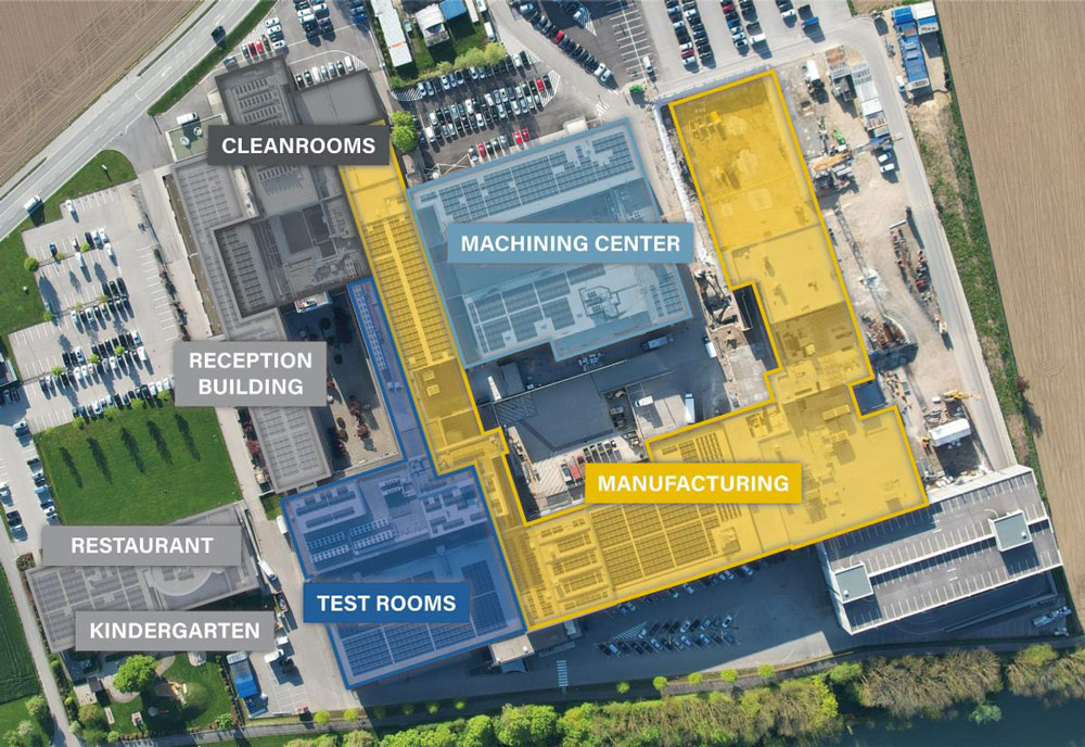
Picture: Overhead view of EVG’s corporate HQ. Source: EVG.
The opening of the Manufacturing V facility follows the company’s previous expansion phase, Manufacturing IV (completed at the end of last year), which itself added nearly 1800m2 of production space and additional warehouse space. Since embarking on these two most recent growth phases, EVG has expanded its production capacity by more than 60%.
Manufacturing VI, EVG’s next phase of expansion that provides for an additional 1400m2 of production and an equal amount of warehouse space, is already under construction, with completion scheduled for second-half 2024.
“New applications fueling the semiconductor industry, such as AI, high-performance computing and autonomous driving, require massive innovations in advanced packaging,” says Dr Werner Thallner, executive operations & financial director and member of the executive board. “As key process enablers for 3D/heterogeneous integration, fusion and hybrid bonding have been transformed into the new scaling mechanism for semiconductor manufacturing. EVG is at the forefront in developing fusion and hybrid bonding and other process solutions that our customers need to support their current and future capacity ramps as well as their long-term product roadmaps,” he adds. “The growth in demand for our products over the years has led us to make major investments in expanding EVG’s manufacturing and cleanroom capacity to meet our customers’ evolving needs. We fully expect this demand growth to continue in the years ahead.”
Heterogeneous integration solutions
EVG’s wafer bonding, lithography and metrology solutions enable the development and high-volume manufacturing of technology innovations in advanced packaging — including backside-illuminated CMOS image sensors and other 3D-IC stacked devices — as well as in MEMS and compound semiconductors. Recent breakthroughs in hybrid bonding to address the needs for 3D device integration, wafer bond alignment technology to address future 3D-IC packaging requirements, IR laser release technology to eliminate glass substrates for advanced packaging and enable thin-layer 3D stacking, maskless exposure for fan-out wafer-level packaging (FOWLP), and nanoimprint lithography NIL and resist processing to support wafer-level optics (WLO) manufacturing, are just a few examples of EVG’s technology for heterogeneous integration and wafer-level packaging.
EVG completes construction of Cleanroom V building
EVG establishes Heterogeneous Integration Competence Center
EVG investing €30m to expand capacity at HQ
- SEO Powered Content & PR Distribution. Get Amplified Today.
- PlatoData.Network Vertical Generative Ai. Empower Yourself. Access Here.
- PlatoAiStream. Web3 Intelligence. Knowledge Amplified. Access Here.
- PlatoESG. Carbon, CleanTech, Energy, Environment, Solar, Waste Management. Access Here.
- PlatoHealth. Biotech and Clinical Trials Intelligence. Access Here.
- Source: https://www.semiconductor-today.com/news_items/2023/nov/evg-281123.shtml
- :has
- :is
- 2024
- 3d
- a
- above
- added
- Additional
- address
- Adds
- advanced
- ahead
- AI
- alignment
- already
- also
- amount
- an
- and
- applications
- ARE
- AREA
- AS
- Assembly
- At
- Austria
- autonomous
- been
- board
- bond
- breakthroughs
- Bringing
- Building
- buildings
- by
- Capacity
- Company’s
- Completed
- Completes
- completion
- components
- Compound
- computing
- construction
- continue
- continued
- converted
- Corporate
- Current
- Customers
- Demand
- Department
- developing
- Development
- device
- Devices
- Director
- dr
- driven
- driving
- eliminate
- embarking
- enable
- end
- equal
- equipment
- establishes
- Ether (ETH)
- evolving
- examples
- executive
- existing
- Expand
- expanded
- expanding
- expansion
- expect
- Exposure
- Facility
- few
- final
- financial
- Floor
- floors
- follows
- For
- forefront
- fully
- fusion
- future
- glass
- Group
- Growing
- Growth
- Have
- he
- Headquarters
- high-performance
- hq
- http
- HTTPS
- Hybrid
- ii
- image
- in
- Including
- Increase
- industry
- innovations
- integration
- into
- investing
- Investments
- items
- ITS
- itself
- jpg
- just
- Key
- laser
- Last
- Last Year
- latest
- Led
- long-term
- major
- make
- manufacturing
- Market
- massive
- mechanism
- Meet
- member
- Metrology
- more
- most
- nanotechnology
- nearly
- Need
- needs
- New
- next
- nine
- November
- now
- of
- offer
- Office
- on
- open
- opening
- Operations
- optics
- Other
- our
- over
- packaging
- Parallel
- phase
- plato
- Plato Data Intelligence
- PlatoData
- previous
- process
- processing
- Product
- Production
- Products
- provides
- Ramps
- rapidly
- recent
- related
- release
- require
- Requirements
- resulted
- roadmaps
- Room
- Rooms
- says
- scaling
- scheduled
- semiconductor
- Semiconductors
- sensors
- Series
- serves
- Services
- significant
- since
- Solutions
- Source
- Space
- st
- stacked
- stacking
- strong
- such
- supplier
- support
- Systems
- Technical
- Technology
- Technology Innovations
- test
- than
- that
- The
- their
- These
- this
- to
- Total
- transformed
- two
- under
- us
- View
- Warehouse
- was
- we
- WELL
- which
- with
- Work
- year
- years
- zephyrnet